Expertise in electronic manufacturing: Coating | Etching | Cleaning
The demand for modern electronics continues to increase, with consumers looking for higher performance, smaller dimensions and maximum reliability.
With our advanced vacuum processing equipment, we enable manufacturers worldwide to produce micro- and nanoelectronic devices to the highest standard. Our technologies for thin film coating, dry etching and precision cleaning are essential for applications in smart sensors, high-frequency electronics, power electronics and advanced electronics packaging.
With our deep process expertise, we develop customised solutions for research and industry, such as developing next-generation sensors, improving RF filters, and failure analysis of complex 3D packages.
scia Systems provides technologies and process equipment for various microelectronic applications:
Smart sensor technology
e.g., biotechnology sensors, lab-on-chip systems, GMR, TMR, IR sensors
High-frequency electronics
e.g., BAW, SAW
Cost-efficient power electronics
Advanced Silicon & beyond
- Failure Analysis and Reverse Engineering for Advanced Electronics Packaging
e.g., multichip packages, SiPs, 3D packaging
MEMS Application Notes
Reverse Engineering of IC chip devices
Frequency Trimming of bulk acoustic wave (BAW) filters
Surface Trimming of surface acoustic wave (SAW) filters
Thickness Trimming of POI wafers for RF filters (SAW)
Film Thickness Correction of thin film read/write heads (TFH)
Temperature Compensation for surface acoustic wave wafers (TC-SAW
SENSOR Application Notes
Deposition of GMR Sensors for flexible magnetoelectronics
Etching of Magnetic Multilayers for tunnel-magneto-resistance (TMR) sensors
Etching of Lithium Tantalate for infrared (IR) sensors
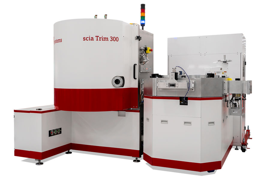
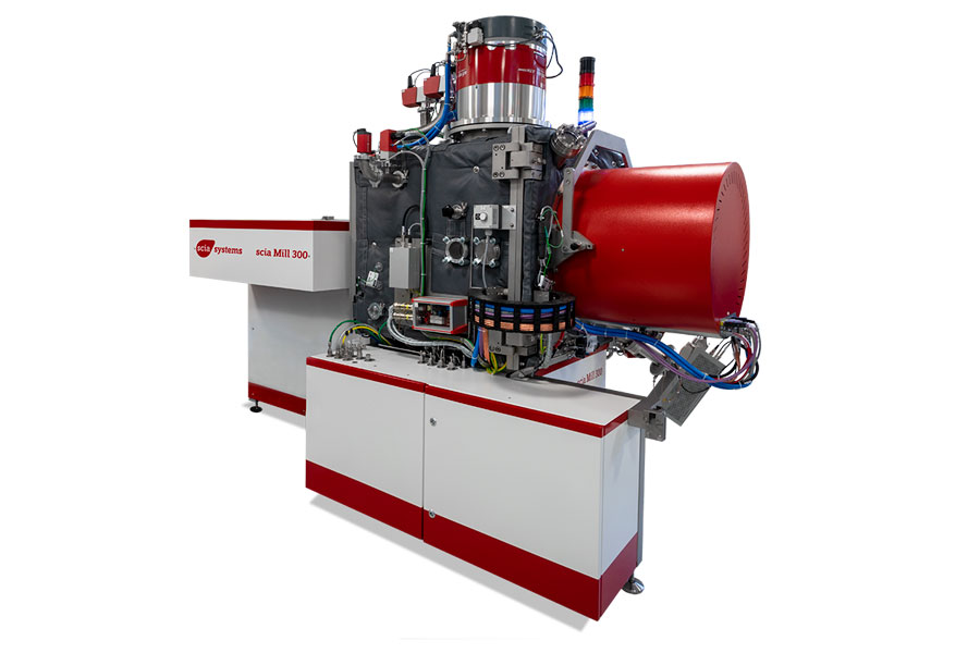
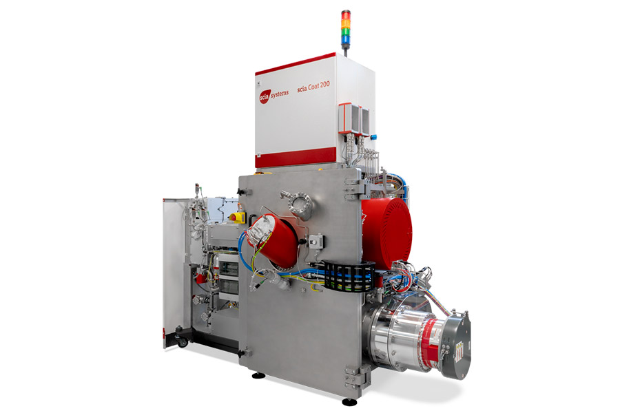
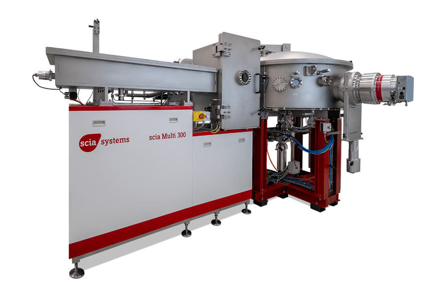
Selected systems for microelectronics production
Learn more
Ion Beam Technology – Enabling an Ever-Evolving Sensor Landscape
In this on-demand webinar, scia Systems’ Sales Director Marcel Demmler explains the principles and advantages of ion beam etching, ion beam deposition, and plasma processing, and how these technologies enable the reliable production of next-generation sensors.
Ion Beam and Plasma Technology for MEMS Production
Our technologies for thin film coating, dry etching and precision cleaning are essential for applications in smart sensors, high-frequency electronics, power electronics and advanced electronics packaging.
Technologies featured in the video:
- Improving RF-filter production by frequency trimming with scia Trim 200
- Ion beam processing of waveguides for Photonic Integrated Circuits (PIC)
- Structuring of micro-optics
- Failure analysis and reverse engineering with precise layer-by-layer material removal
- Enhancing sensor technology with increased sensitivity & energy efficiency
- Structuring of TMR Sensors via ion beam etching
One system for all your processes: scia Cluster 200
Whether you want multiple chambers dedicated to one process or want to combine our wide process know how – we have the ideal cluster-layout for you!
- Ion Beam Trimming (IBT)
- (Reactive) Ion Beam Etching (RIBE)
- (Dual) Ion Beam Deposition (DIBD)
- Magnetron Sputtering (PVD)
- Reactive Ion Etching (RIE)
- Plasma Enhanced Chemical Vapor Deposition (PEVCD)
- Atomic Layer Deposition (ALD)
- Electron Beam Evaporation (EBE)
Ask for your dedicated solution!
scia Systems GmbH
Clemens-Winkler-Str. 6c
09116 Chemnitz
Germany


