Learning: Scientific Content about Thin Film Technology
We want to support the continuous development of plasma and ion beam technology, so we share our knowledge. The learning portal of scia Systems offers scientific insights for both beginners and experts. If you have any questions or need more information on any topic, please do not hesitate to contact us.
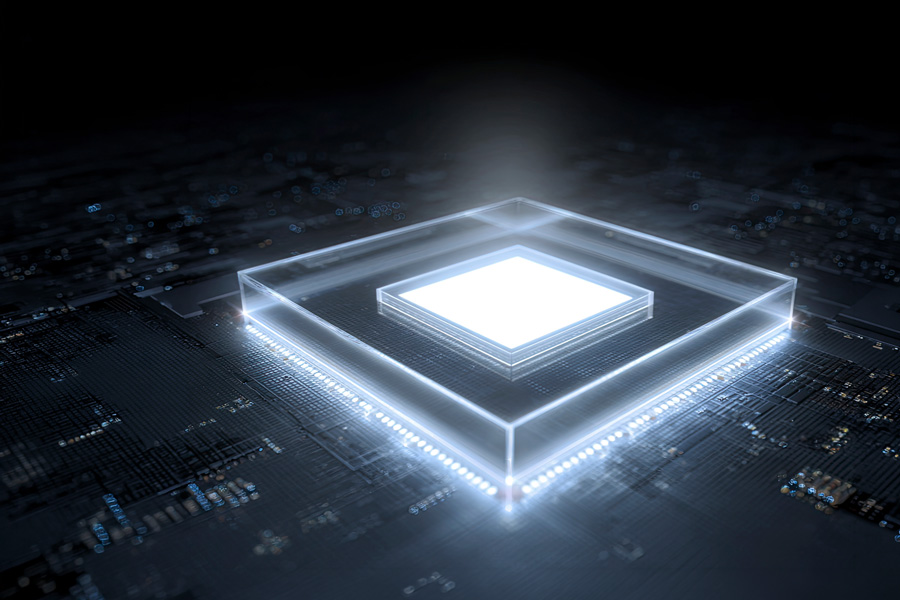
Reactive Ion Beam Etching of Lithium Niobate for Photonic Integrated Circuits
Video presentation on how RIBE addresses sidewall effects such as footing, fencing, and trenching in LiNbO3 and TFLN processing.

Ion Beam Technology – Enabling an Ever-Evolving Sensor Landscape
Webinar on how ion beam technology ensures accuracy, scalability, and reliability in the production of modern sensors.

Structuring and Uniformity Improvement of Thin Film Waveguide Materials
Video presentation that covers specific applications in nanodevice and thin-film manufacturing with materials like Lithium Niobate and Silicon Nitride.
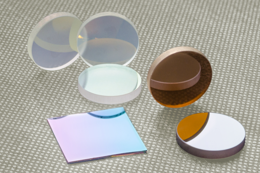
Overview of PVD Technologies
Comparison of ion beam sputtering, magnetron sputtering and evaporation.

Ion beam technology for frequency filters in mobile communication
In every cell phone are components that have been manufactured on the production lines of scia Systems.

Ion beam technology for thin piezoelectric films
Video presentation: The advantages of ion beam technology for piezoelectric layers.

Advanced Patterning for Slanted Surface Relief Gratings
Video presentation: Methods to create optical gratings with constant or variable slant angle
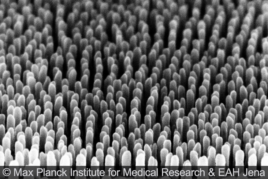
Reactive ion etching of anti-reflective nanostructures
Moth-eye effect on substrates up to 300 mm and on 3D-Objects.
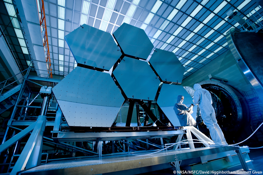
Ion beam figuring for telescope mirrors
Video presentation: surface error correction under high vacuum conditions.
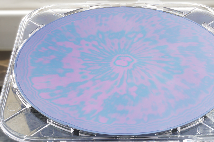
Ion beam trimming of POI wafers
Video presentation: Surface correction of piezoelectric materials
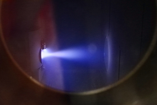
The Technology of Ion Beam Figuring
Etching with extremely high precision especially for optical substrates

Ion beam etching for optics structuring
Video presentation: How to structure your optics with reactive ion beam etching.

Direct etching of slanted gratings
Video presentation: Etching of SRG used as in- and out-coupler in waveguides.
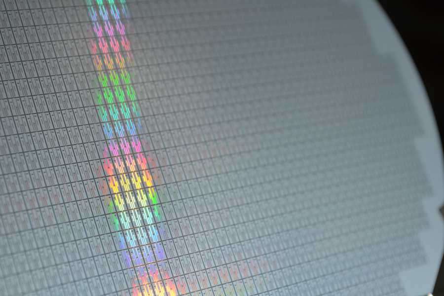
Magnetron Sputtering of silicon dioxide
Advantages of magnetron sputtering for SiO2 deposition

Slanted gratings by ion beam trimming
Video presentation: Processing of optical gratings with varying slant angles by reactive IBT
Additional Information
Technology Overview
Ion beam and plasma processes for etching, coating and cleaning of substrates.
Application Notes
Selected applications for MEMS, optics and sensors, presented in detail.