Reactive ion etching of anti-reflective nanostructures with moth-eye effect on 3D surfaces
In many areas of modern optical technology, a reflective effect is unwanted. The conventional method of reducing reflection on a surface is to apply one or more additional thin layers with a thickness of up to a few µm. Compared to other options, using anti-reflective nanostructures on optical substrates provides multiple physical benefits, including no constructive interference effects, minimal dependence on the angle of incidence and wavelength of the radiation as well as the avoidance of possible layer ablations. It is also potentially more economically attractive to produce anti-reflective nanostructures compared to the production of multilayer coatings.
These properties lead to a need in the modern optics industry to develop processes for nanostructuring and high-end antireflection coatings not only for plane substrates but also for voluminous, spherical, and aspherical lenses.
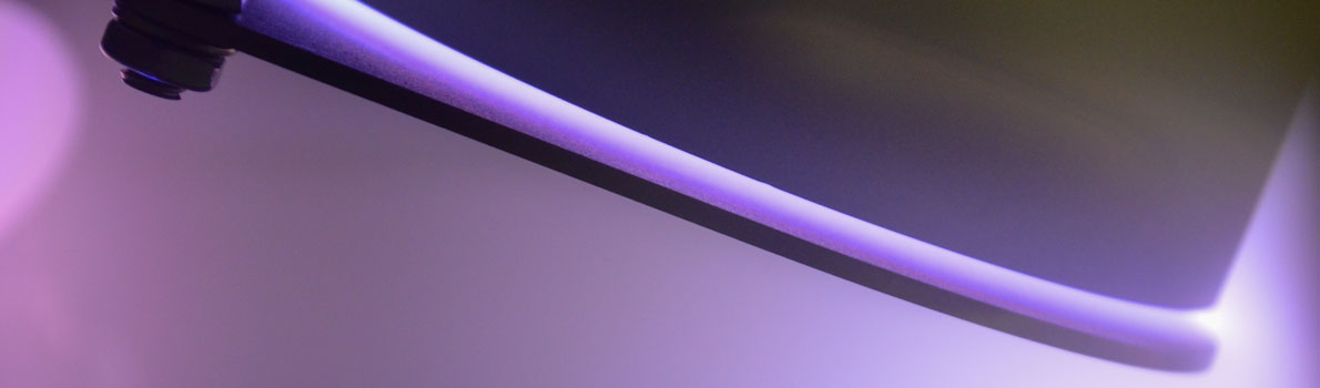
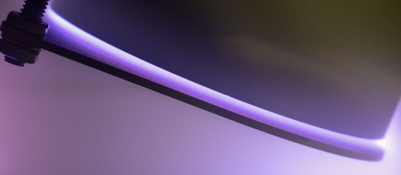
As part of the "arivo3d" project, a new kind of nanostructured surfaces is being developed at the Ernst Abbe University of Applied Sciences Jena: Inspired by nocturnal insects, in particular moths, the new cone-shaped anti-reflective nanostructures aim to achieve a broadband anti-reflection coating without relying on conventional thin films.
scia Etch 300 as a key to the production of advanced optical surfaces
The EAH Jena uses a scia Etch 300 to produce these structures, enabling plasma etching. The system uses a special reactive ion etching (RIE) process on substrates up to 300 mm in diameter and on highly curved, voluminous, three-dimensional objects such as lenses, mirrors, and prisms. This will push forward research in the field of nano-optics and significantly accelerate the development of anti-reflective nanostructures.
We wish the EAH Jena every success with their project and are already looking forward to many exciting research results.
Website of the University of Applied Sciences Jena: www.eah-jena.de

SEM image of artificially produced anti-reflective moth-eye structures on quartz glass.
© Max Planck Institute for Medical Research & EAH Jena

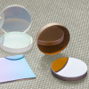
Reflection on fused quartz - the left side is processed on both sides, and the right side is unprocessed.
Technology

Learn more about reactive ion etching and other ion beam and plasma processes in our technology overview.
Application

In our Application Note we show you, how ion beam sputtering can be used for for High- and Anti-Reflective Coatings
Product

The scia Cluster 200 is the ideal system for all your processes with high flexibility and best usability on wafers up to 200 mm.
Do you want to speak to one of our experts? Contact us:
scia Systems GmbH
Clemens-Winkler-Str. 6c
09116 Chemnitz
Germany
Tel: +49 371 33561-0
✉ sales@scia-systems.com
Additional Information
Overview of PVD Technologies
Comparison of ion beam sputtering, magnetron sputtering and evaporation.
Ion beam trimming of POI wafers
Video presentation: Surface correction of piezoelectric materials