
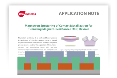
New App-Note: Magnetron Sputtering of Contact Metallization for TMR Devices
scia Systems, based in Chemnitz, Germany, develops and manufactures high-end equipment for ultra-precise surface processing using advanced ion beam and plasma technologies. The systems are designed for coating, etching, and cleaning with nanometer accuracy. scia Systems stands for perfection at the nanometer scale. Since its foundation in 2013, scia Systems has established itself as a technology leader in thin-film processing. The equipment is known for its reliability, flexibility, and performance, tailored to the specific needs of high-volume production and research applications.
scia Systems offers a wide range of ion beam and plasma process equipment that enables our customers to design new and innovative products with unique functional properties. Machines made by scia Systems have been successfully implemented in various high-tech industries worldwide, including microelectronics, MEMS, and precision optics industries.
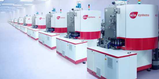
Our systems are flexible and modular in design. This enables us to offer standard as well as individual solutions for our customers.

Our equipment is mainly used in the production of MEMS and precision optical components, but also in astronomy and biomedical technology.
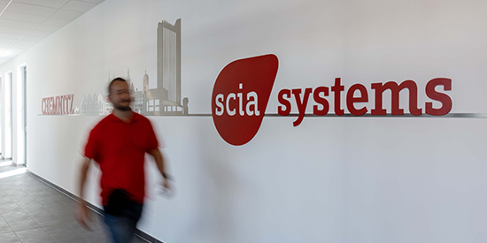
Pushing the latest technologies with ambition and constantly evolving - that's what scia Systems is all about.



2026-10-13 to 2026-10-15
San Francisco, USA
Booth: 3303 South Hall (Floorplan)
Partner on Site: AARD Technology

2026-11-03 to 2026-11-04
Eindhoven, Netherlands
Partner on site: Benelux Process

2026-11-10 to 2026-11-13
in Munich, Germany
Booth: B1-909 (Floorplan)
scia Systems GmbH
Clemens-Winkler-Str. 6c
09116 Chemnitz
Germany
Tel: +49 371 33561-0