
Ion beam sputtering: Dense and high-precision coatings for advanced applications
Ion Beam Sputtering (IBS), also known as Ion Beam Deposition or Ion Beam Sputter Deposition (IBSD), is a PVD technology that produces especially dense, uniform and defect-free thin films on a substrate.
A focused broad ion beam bombards the target material with noble gas ions, such as argon or nitrogen. The ions collide with the surface of the target with high kinetic energy, ejecting individual particles (atoms or molecules) of the material and causing them to condense on a substrate surface to form a thin coating. By using various targets in one process chamber, multiple stacked layers, so-called multilayer coatings, can be produced with a high quality.
Compared to other PVD technologies like magnetron sputtering or evaporation, ion beam sputtering offers several advantages. The sputtered particles hit the substrate with high energy. Due to this, they have a high surface mobility and easily embed themselves between already deposited particles, resulting in particularly dense and defect-free layers. The low sputtering pressure and low process temperatures allow dense film growth and excellent film properties. In addition, the ion beam energy is precisely adjustable, allowing greater control over the properties of the deposited layer, including density, adhesion, and composition.
A special form of ion beam sputtering is dual ion beam sputtering or dual ion beam deposition. By adding an assist ion beam source, a second ion bombardment is used to influence the growing film on the substrate or pre-clean the substrate.
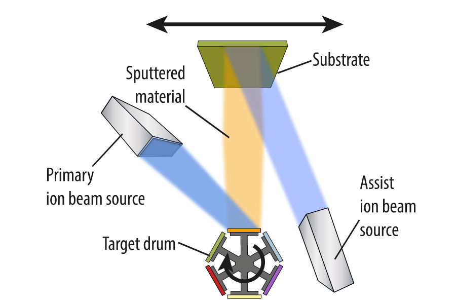
Dual Ion Beam Sputtering in scia Coat 500
Ion Beam Sputtering Systems
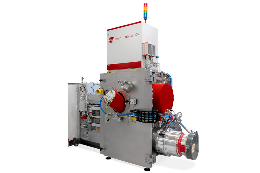
scia Coat 200 - Multilayer Deposition on wafers up to 200 mm
- Ion Beam Sputtering (IBS)
- Dual Ion Beam Sputtering (DIBS)
- Ion Beam Etching (IBE)
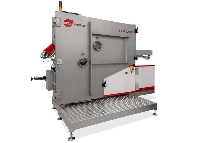
scia Coat 500 - Large Area Multilayer Coating for Precision Optics
- Ion Beam Sputtering (IBS)
- Dual Ion Beam Sputtering (DIBS)
- Ion Beam Etching (IBE)
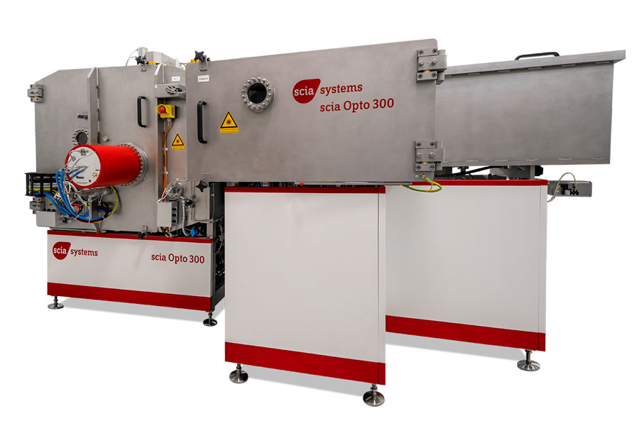
scia Opto 300 - Coating of Precision Optics up to 300 mm dia.
- Ion Beam Sputtering (IBS)
- Dual Ion Beam Sputtering (DIBS)
Applications
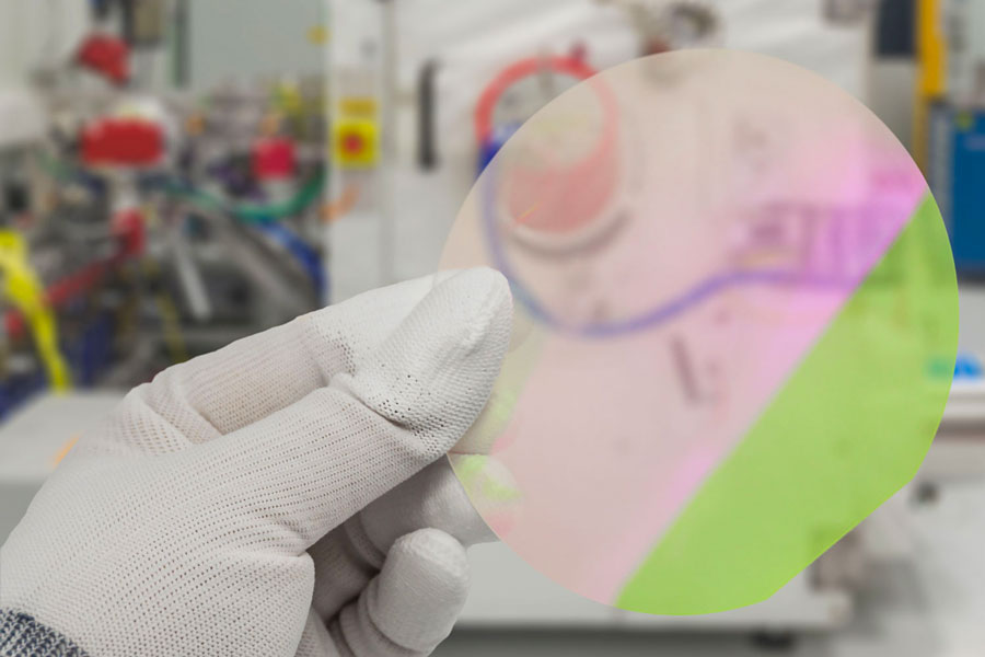
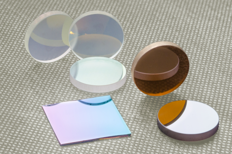
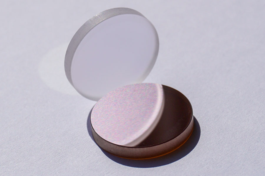
Ion beam sputtering is used in various applications. For instance, in MEMS industry it is used to generate piezoelectric coatings for advanced mobile communications. It is also used in the optics industry to create coatings on lenses or mirrors to optimize their reflectivity or transmittance for certain wavelengths. Furthermore, ion beam sputtering is used in the production of wear resistant coatings and many other areas where precise thin films are required
Application Note: Dielectric Coatings
Ion Beam Sputter Deposition of Dielectric Films on Large Optical Substrates.
Overview of PVD Technologies
Comparison of ion beam sputtering, magnetron sputtering and evaporation.
Application Note: HR and AR Coatings
Ion Beam Sputtering for High- and Anti-Reflective Coatings

Ion beam technology for thin piezoelectric films
Video presentation: The advantages of ion beam technology for piezoelectric layers.
More Information
- Not the right system yet? See our complete portfolio.
- Overview of Ion Beam and Plasma Processing Technologies
- Tailor Made Solutions
- Contact
