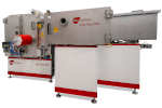
Overview of PVD Technologies
Physical vapor deposition (PVD) describes various coating processes through condensation of vaporized material to create thin films on a substrate. All processes are vacuum-based. We like to introduce three kinds of processes: ion beam sputtering, magnetron sputtering and evaporation. Each technology has different advantages, below we give you a short overview:
Ion Beam Sputtering
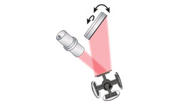
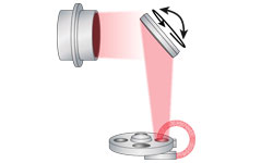
Ion Beam Sputtering (IBS) / Ion Beam (Sputter) Deposition (IBD)
An ion beam is facing a target. The resulting ion bombardment physically removes material from the target which is deposited on the substrate surface. The adding of reactive gases such as oxygen allows reactive ion beam sputtering of e.g. dielectric materials.
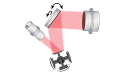
Dual Ion Beam Sputtering (DIBS) / Dual Ion Beam (Sputter) Deposition (DIBD)
By adding an assist ion beam source an extra ion bombardment at the substrate can be introduced. This is used to influence the growing film or pre-clean the substrate.
Advantages
- Ion beam energies exactly adjustable with small energetic distribution
- Kinetic energies of sputtered particles (neutral target atoms) in the range of several 10 eV (10 x higher than magnetron sputtering or evaporation)
- High surface mobility of condensing particles leads to smooth and defect free films
- Low sputtering pressure and low process temperatures enable dense layer growth and outstanding layer properties
- Additional densification and modification (e.g. oxidation) by assist ion beam source
- Easy in-situ target change, due to multiple materials on a rotational holder
Application Examples
- Ion Beam Sputtering of Dielectric Films on Large Optical Substrates
- Ion Beam Sputtering for High- and Anti-Reflective Coatings
Ion Beam Sputtering Systems

scia Coat 200
for high quality multilayer
deposition on up to 200 mm

scia Coat 500
for large area multilayer deposition on up to 500 mm x 300 mm
scia Opto 300
for high precision optical coatings on up to 300 mm dia.
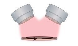
Magnetron Sputtering
Magnetron sputtering uses a cathode with a permanent magnetic field to excite a dense plasma at the cathode surface. The target material, placed at the cathode surface, is physically sputtered by ion bombardment and gets deposited on the substrate surface. Thereby several process arrangements lead to different layer properties.

Sputtering with Single Magnetron
The process chamber contains one magnetron with rotating magnetic field with a target diameter larger than the substrate diameter. The arrangement allows thin films with high troughput.
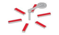
Confocal Sputtering
The sputter arrangement consists of up to 4 Magnetrons, each with target diameter smaller than substrate diameter.The magnetrons can be combined for co-sputtering of alloys (different target materials) or for bipolar sputtering (same target materials). In order to achieve a homogeneous material mix on the substrate surface, a sufficiently fast substrate rotation is required.
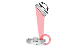
Dynamic Sputter Deposition
The rotating substrate is moved linearly or orbitally over rectangular magnetrons to produce multilayer coatings. The individual emission profiles of the magnetrons are compensated by pre-calculation of the movement profiles, the layer thickness can be controlled by speed variation.
Advantages
- High deposition rate
- Good process repeatability for multilayers with uniform thickness
- Optional pretreatment with additional ion beam source (for dynamic sputter deposition)
- The low energy of the sputtered particles leads to smooth surfaces
Application Examples
Magnetron Sputtering Systems

scia Magna 200
for advanced wafer coatings
of up to 200 mm

scia Multi 300
for uniform multilayer deposition on wafers up to 300 mm dia.

scia Multi 500
for multilayer coating of large optics up to 500 x 300 mm

scia Multi 680
for multilayer coating of large
substrates up to 680 mm

scia Multi 1500
for multilayer coating of large
substrates up to 1500 mm
Evaporation
Electron Beam (E-Beam) Evaporation
Current through a tungsten filament causes an electron emission, which is unified and accelerated to an electron beam by high voltage. A magnetic field deflects the e-beam so that it is focused into the crucible. The material in the crucible is bombarded with that e-beam and evaporates to a gaseous state for deposition on the substrate to be coated.
E-Beam Evaporation with Ion Beam Assistance
The electron beam evaporator is equipped with an additional ion beam source to pre-clean the substrate.
Advantages
- High deposition rates for evaporation of high temperature materials and refractory metals
- Stress optimized process design with medium layer density (with assist ion beam source)
- Deposition of films with nearly the same purity as the target material
- Water cooled crucible for controlled evaporation of target material and to avoid unwanted contamination
Electron Beam Evaporation System
scia Eva 200
Glancing Angle Deposition for precise nano-structures on wafers up to 200 mm
Summary
The highest precision in PVD-coating is achieved with ion beam sputtering. Especially in the sectors of microelectronics and precision optics, the demands on accuracy and density of the layers to be produced are so high, that a production using evaporation processes is no longer possible.
To ensure a high yield of functional devices, technologies such as magnetron sputtering and ion beam sputtering are therefore required. However, these methods have a lower throughput and are more expensive to purchase and to operate. If a coating process for high temperature materials with high deposition rates is needed, E- Beam Evaporation is a more cost-effective alternative.
Here you can find an overview of the advantages and disadvantages of the PVD technologies presented:
Ion Beam Sputtering
Pro
- Highest coating precision
- Processing with low substrate temperature
- Dense and very pure films
Con
- High investment price
- Low deposition rates
- High complexity
Magnetron Sputtering
Pro
- High coating precision
- Processing with moderate substrate temperature
- Dense films
Con
- High film stress
- Medium deposition rates
- Formation of droplets possible under unfavorable conditions
E-Beam Evaporation
Pro
- High deposition rates
- Stress optimized films with medium density
Con
- Heating required
- Thermal influence on substrate
scia Systems offers high-quality solutions for wafer-based E- Beam Evaporation with Ion Beam Assistance, different Magnetron Sputtering arrangements and advanced Ion Beam Sputtering processes. Our wide range of vacuum process equipment is flexible and modular. This means that our systems can be configured for high volume production environments as well as research applications.
Our team will be happy to help you find the optimal technology and system configurations for your manufacturing needs. Please contact us for more information:
scia Systems GmbH
Clemens-Winkler-Str. 6c
09116 Chemnitz
Germany
Tel: +49 371 33561-0
✉ sales@scia-systems.com
Additional Information
Magnetron Sputtering of SiO2
Advantages of magnetron sputtering for silicon dioxide deposition.
Product Portfolio
Discover our equipment for coating, etching and cleaning processes.