Research Projects
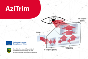
AziTrim: scia Systems develops an innovative process chain for the Production of SRG
2026
scia Systems GmbH is partner in the funded joint project AziTrim, a research initiative aimed at developing an optimized process chain for the fabrication of variably tilted surface relief gratings (SRGs) using ion beam etching.

MultiALD research project develops innovative processes for ultra-thin aluminum-based coatings
2025
The research project "System and process development for the atomic layer deposition of aluminum-based thin films for barriers, actuators, and electronics – MultiALD" is working on new methods to produce thin films based on trimethylaluminum (TMA) using atomic layer deposition (ALD).

Participation in the joint project MOBBS
2024
The joint project „Monolithische Binär- und Blaze-Gitter auf Silizium und Oxiden (MOBBS)” brings together ZEISS Jena GmbH, IOM Leipzig, and scia Systems GmbH to develop ion-beam-based production processes for manufacturing various optically active grating structures on silicon and oxides.
Blazed diffraction gratings – also known as Echelette gratings – are essential components in spectrometers and high-performance beamlines. Tilted binary structures enable the coupling and decoupling of light, as well as its precise manipulation, in smart glasses. However, these blazed structures cannot be fabricated using lithography on silicon substrates, as silicon is not transparent at the required exposure wavelengths. Binary structures for light guides in smart glasses are currently manufactured primarily in a perpendicular orientation. However, the performance of such a light guide can be significantly improved by using slanted binary structures.
In the project, reactive ion beam etching is used to produce precise monolithic, etched silicon diffraction gratings for beamline applications in the VUV, EUV, and X-ray ranges, as well as slanted binary gratings for targeted light guidance in smart glasses.

scia Systems contributes to the research of piezoelectric materials and devices
2023
In the new "Christian Doppler Laboratory" at TU Wien, research is focused on the fundamental issues of piezoelectric materials and devices to enable future applications. We are proud to support the new laboratory with a scia Coat 200 as an industrial partner. This ion beam sputtering system will be used to produce extremely precise, smooth, and uniform coatings on substrates, including advanced materials such as aluminum nitride and scandium aluminum nitride.

Joint project for 3-nanometer microelectronics research – PIn3S
2022
The PIn3S project focuses on the development of process and equipment technology for the production of adaptive optics, which are required for semiconductor technology with conduction path distances of only 3 nanometers. We are proud to contribute our know-how and experience in ion beam and plasma technology to this project ...
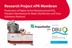
Participation in the joint project nPK-Membran
2029 – 2022
As part of the joint project “Production of Highly Active Nanostructured TiO₂ Filtration Membranes for Water Disinfection and Trace Substance Removal (nPK Membrane),” the Fraunhofer Institute for Ceramic Technologies and Systems (IKTS) and scia Systems GmbH collaborated to develop photocatalytically active microfiltration membranes for water treatment.
Clean drinking water is one of our most important resources. However, the water cycle is increasingly being contaminated by anthropogenic micropollutants, as well as by fertilizers, chemicals, and medications. Photocatalysis using titanium dioxide (TiO2) breaks down such contaminants into CO2 and water without leaving any residue.
By firmly bonding a nanostructured TiO₂ layer to a ceramic microfiltration membrane, a component is created that combines filtration and photocatalytic degradation in a very small space and can be expanded into scalable membrane stacks. In this project, scia Systems was responsible for depositing TiO₂ layers via magnetron sputtering, as well as depositing undoped titanium layers onto the microfiltration membranes via ion beam sputtering (IBS). The most successful process route was a combination of magnetron sputtering followed by electrochemical oxidation and heat treatment: the nPK membranes produced this way showed competitive photocatalytic degradation rates and excellent layer adhesion, even under thermal stress.

Successful development in research project HiPERFORM
2021
With the substrate holder designed by scia Systems, epitaxial Aluminum Nitride (epi-AlN) can now be deposited on silicon (111). This is an important step for the development of GaN-based switch technologies. As these have up to 30% less energy losses compared to existing architectures, they can be used to produce more affordable and efficient electric and hybrid vehicles.

ENAL: Nano Anti-Wear Coatings for Precision Micro Cutting Tools
2019
The ENAL project (Use of Nanocoated Tools in Printed Circuit Board Manufacturing) aims to develop a new generation of microfabrication tools based on nano-wear-resistant coatings for use in printed circuit board manufacturing.
Building on the joint project “NanoTools”—in which Al₂O₃ coatings on drills achieved up to a sixfold increase in tool life—dual ion beam deposition (DIBD) is used to deposit nanocoatings onto the cutting surfaces of mechanical tools. The goal is to extend the life of the drill bits without compromising the quality of the drilling process or the final product.

Participation on cooperative project – ALMET
2019
Together with project partners scia Systems is working within the ALMET project on the development of systems and processes for the atomic layer deposition of metallic thin films (mALD). The objective of the project is the conformal deposition of copper and cobalt thin films within an industrial-suited ALD reactor. The reactor allows plasma assisted ALD (PALD) by a special chamber-in-chamber layout and enables a variety of different ALD processes. scia Systems is pleased to support the project with its experience and know-how.

Participation on research project – HiPERFORM
2018
Together with 30 project partners from 8 European countries scia Systems is working on the HiPERFORM - project to introduce wide band-gap power electronics in the drivetrain of electric vehicles. The main research objectives of the project are: cost reduction, energy efficiency, and less volume of the devices. Research will focus on both new materials and improved manufacturing processes, such as the cost-effective deposition of gallium nitride (GaN) by magnetron sputtering. The topic of scia Systems is the development of a substrate holder which meets the special requirements regarding temperature and process time.
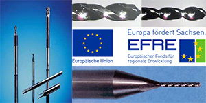
Participation on joint research project – NanoTools
2017
scia Systems participates in a joint project to develop coated micro cutting tools based on nano wear-protection layers. The objective of the collaboration between industrial companies and R&D institutes is to provide a scientific-technical base for the reliable industrial use of ALD coatings (ALD - atomic layer deposition) and ion beam coatings (DIBD – dual ion beam deposition), in comparison to PVD coatings, as well as to define their field of application.
Participation on joint project – DANAE
2017
Together with the project partners scia Systems is working on the development of thin film and matching technologies for nanoscale acousto-electronics. The objective of the collaboration is to establish the pre-conditions for depositing and trimming of materials needed in the acousto-electronic industry as well as the development of required components. The topic of scia Systems is: trimming technologies and the development of components for manufacturing of nanoscale acousto-electronic devices.
Additional Information
Technology Overview
Ion beam and plasma processes for etching, coating and cleaning of substrates.
Application Notes
Selected applications for MEMS, optics and sensors, presented in detail.