Ion Beam Etching: Precise Processing of Complex Surface Structures
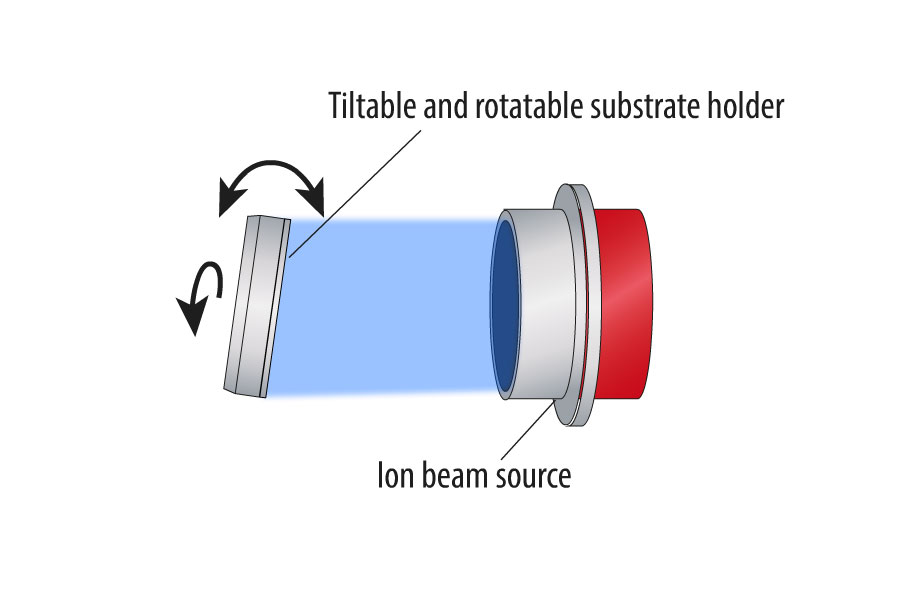
Ion Beam Etching (IBE), also referred to as Ion Beam Milling (IBM), is a highly precise method for surface processing. A broad beam of positively charged ions (typically argon ions) is accelerated onto a substrate. Thereby, the ions transfer their kinetic energy to the surface atoms, causing them to be ejected and thus removing the material. To achieve a uniform and accurate etching result, the substrate is rotated during the process, while the ion beam has a larger diameter than the substrate.
Advantages of Ion Beam Etching:
- High precision - by etching under a defined angle of incidence and adjustable ion energy, even complex structures can be created with high accuracy.
- Low substrate temperature, which minimizes heat-induced deformation or damage to the material.
- High versatility: Ion beam etching is suitable for a wide range of materials, including metals, semiconductors, polymers, and ceramics.
- Surface cleanliness: oxide layers or other contaminations can be removed from the surface.
Special forms of ion beam etching are Reactive Ion Beam Etching (RIBE) and Chemically Assisted Ion Beam Etching (CAIBE), where reactive gases are used in addition to inert gas, e.g., to increase selectivity, to influence trench angles or to enhance etch rates.
Process of Ion Beam Etching
Equipment for Ion Beam Etching
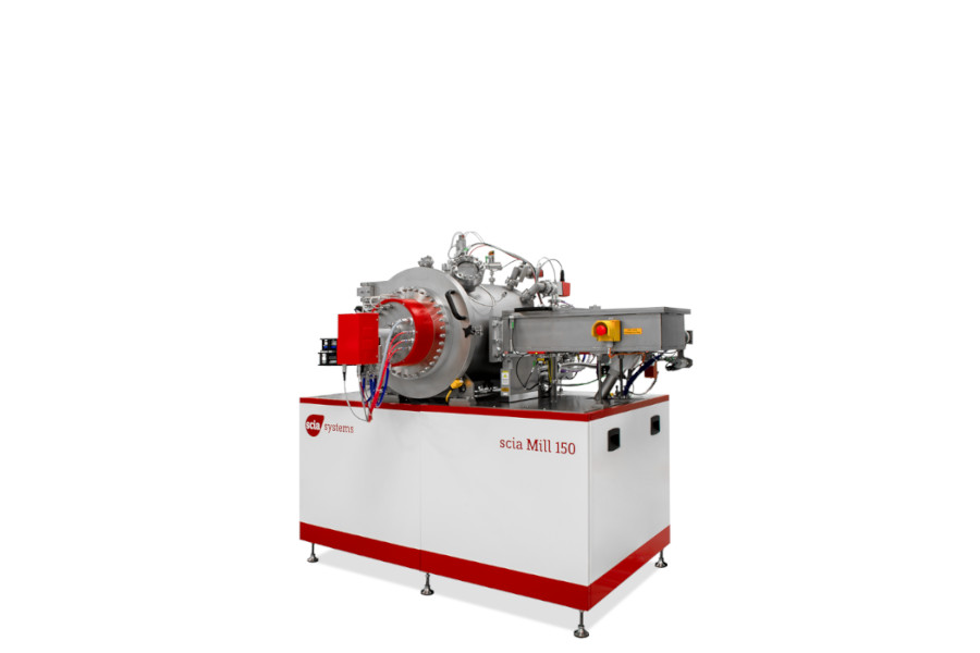
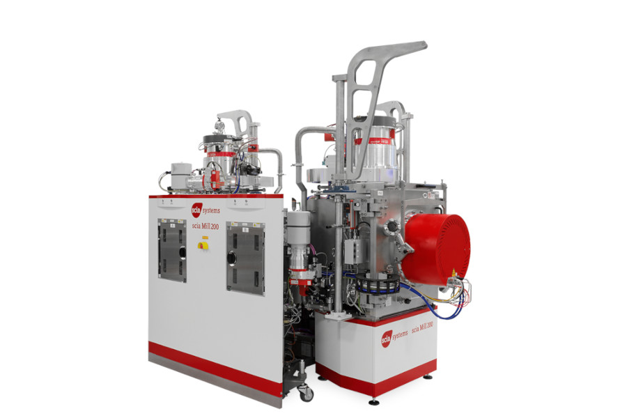
System for small scale production and R&D applications of substrates up to 150 mm
- Ion Beam Etching
- Reactive Ion Beam Etching
- Chemically Assisted Ion Beam Etching
Fully production proven system for mass production of wafers up to 200 mm
- Ion Beam Etching
- Reactive Ion Beam Etching
- Chemically Assisted Ion Beam Etching
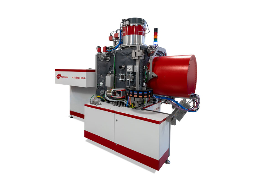
Full surface etching system for wafers up to 300 mm
- Ion Beam Etching
- Reactive Ion Beam Etching
- Chemically Assisted Ion Beam Etching
Applications
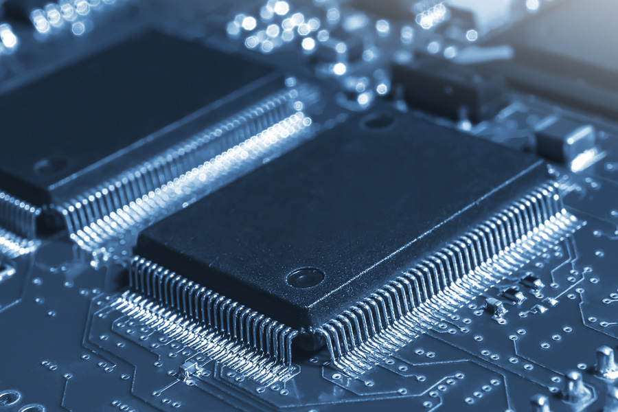
Ion beam etching is used in the MEMS industry for etching various metals (Au, Ru, Ta, ...) and dielectric materials as well as for patterning of microchips. It also enables high-precision processing of optical components such as lenses, filters, and mirrors. Furthermore, it can be used for the fabrication of 3D-optoelectronic microstructures and other photonic structures such as waveguides and gratings (e.g., slanted relief gratings for AR applications).
Another important application of ion beam etching is the modification of surfaces to improve the adhesion of coatings, the creation of textured surfaces and the removal of contaminations.
Application Note: Reverse Engineering of IC chip devices
Precise and uniform delayering by ion beam etching.
Application Note: Magnetic Multilayers for tunnel-magneto-resistance sensors
Removal of all materials of the TMR stack with the help of ion beam milling.

Application Note: Surface Relief Gratings for AR- and MR-Devices
Reactive ion beam etching of slant angles as flat as 60 degree.
Application Note: Manufacturing of ultra-thin Lithium Tantalate for IR Sensors
Layer thickness reduction by ion beam etching.
More Information
- Not the right system yet? See our complete portfolio.
- Overview of Ion Beam and Plasma Processing Technologies
- Tailor Made Solutions
- Contact
