Ion Beam Etching for Manufacturing of Ultra-Thin LT for IR Sensors
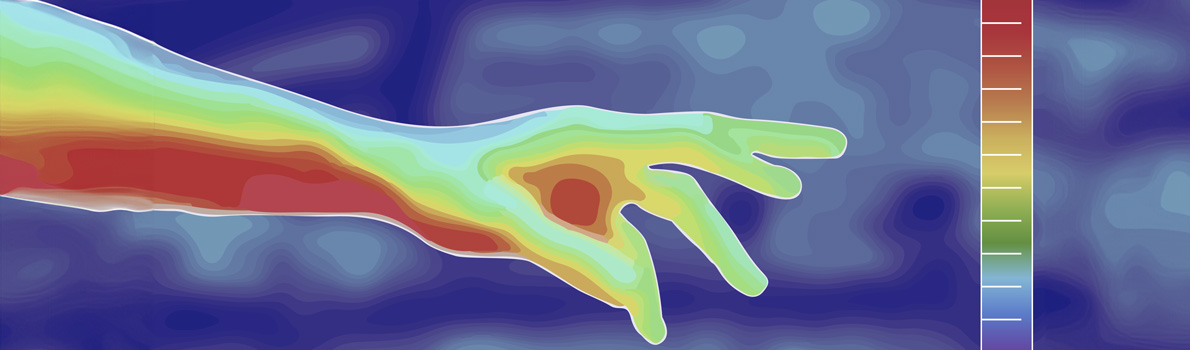
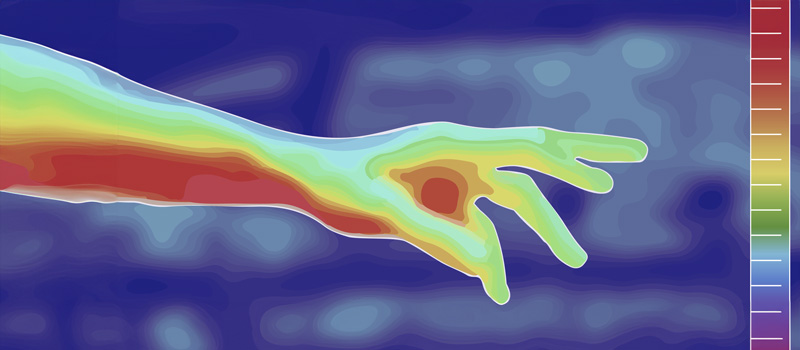
High-sensitivity sensors for radiation detection in the infrared (IR) range have a wide field of application e.g. for detectors in IR spectroscopy or contact-free temperature measurement. A common material for those sensors is pyroelectric lithium tantalate (LT).
To achieve an optimum sensor performance, a reduction of the thermal inertial, and hence the thickness of the lithium tantalate is required. Classical slicing, based on a grown single crystal of a certain diameter, works down to a thickness of 300 µm, which can be further decreased to about 25 µm by using chemical mechanical polishing (CMP). Achieving a smaller thickness of the LT substrate is not possible due to the probability of crack formation, which dramatically increases at this point. The method of choice for further minimizing LT thickness in order to increase D* is Ar+ ion beam etching, also known as ion beam milling.
...
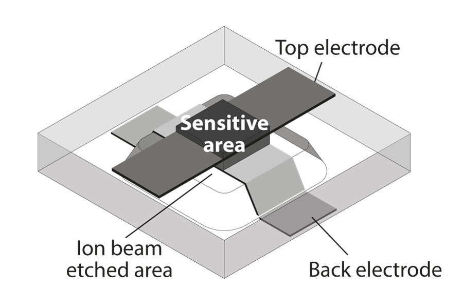
Fig. 1: Sketch of the integration of the LT sample (ion beam etched area) in a pyroelectric sensor.
Reach out
Please contact us for further information.
Related Information
Related Products: scia Mill 150 & scia Mill 200 & scia Mill 300
- Full substrate ion beam milling with superior uniformity
- Etching with inert gases to avoid after-corrosion
- Thinning of materials like LT beyond the limits of CMP
- Stable process over tens of hours for removal of several µm of material
- Helium backside cooling contact for substrates allows to use photoresist
- Reactive gas compatibility in RIBE and CAIBE processing
- Ion beam source with high stability, adjustable ion energy and ion current density
- Complete software integration and automated processes via recipe
