
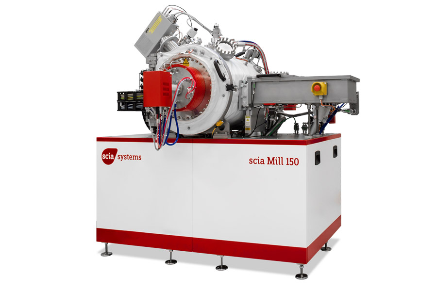
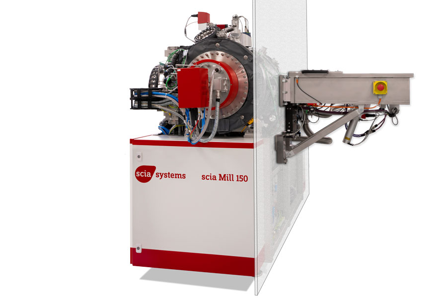
Substrate size (up to) | 150 mm dia. |
Substrate holder | Water-cooled, helium backside cooling contact, substrate rotation 1 to 20 rpm, tiltable in-situ from 0° to 165° in 0.1° steps |
Ion beam source | 190 mm circular microwave ECR source (MW218-e) |
Neutralizer | Triple plasma bridge neutralizer (N-3DC) |
Base pressure | < 5 x 10⁻⁷ mbar |
System dimension (W x D x H) | 1.90 m x 1.80 m x 1.75 m (without electrical rack) |
Configurations | Single chamber, optional single substrate load lock, optional OES or SIMS based end point detection |
Software interfaces | SECS II / GEM, OPC |
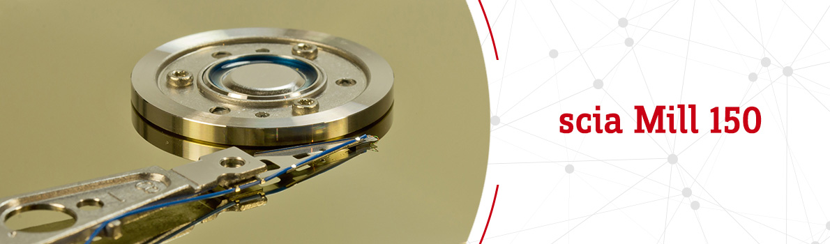
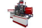
Full Surface Ion Beam Etching on 150 mm Substrates
The scia Mill 150 is designed for structuring of complex multilayers of various materials. With its fully reactive gas compatibility the system also enables reactive etching processes with enhanced selectivity and rate. Due to its space saving design the scia Mill 150 is ideal for small scale production and R&D applications.
Features & Benefits
- Etching angle adjustment with tiltable and rotatable substrate holder
- Excellent uniformity without shaper
- Enhanced selectivity and rate with reactive gases
- Process control with exact SIMS based or optical end point detection
- Carrier concept for adaptation to variable substrate sizes
- Processing of wafers with photoresist masks due to good wafer cooling
Applications
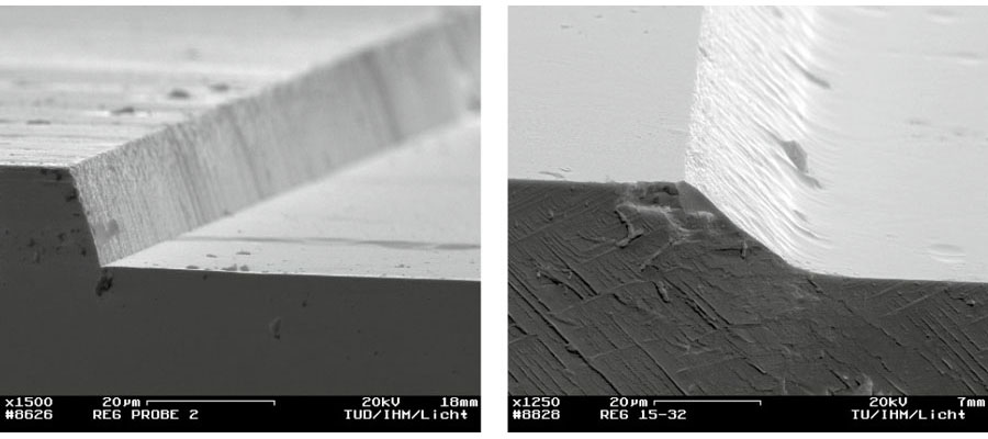
SEM pictures of etching edge with courtesy of DIAS Infrared GmbH.
Etching of 15 µm lithium tantalate with photoresist and 15° angle of incidence for a pyroelectric sensor.
Left: Standard photoresist mask with sharp edges.
Right: Optimized photoresist with smooth edges improves electrical bonding of the sensor.
- Structuring of magnetic memory (MRAM) and sensors (GMR, TMR)
- Milling of metals in MEMS production (Au, Ru, Ta, …)
- Milling of multilayers of different metal and dielectric materials
- Chemically Assisted Ion Beam Etching (CAIBE) of compound semiconductors (GaAs, GaN, InP, …)
- Production of 3-dimensional optoelectronic microstructures
- Ion beam smoothing for reduction of microroughness
- Reactive Ion Beam Etching (RIBE) for pattern transfer for optical gratings (SiO2)
Application Notes
- Surface Relief Gratings for AR- and MR-Devices
- Magnetic Multilayers for tunnel-magneto-resistance (TMR) sensors
- Manufacturing of ultra-thin Lithium Tantalate for IR Sensors
- Reverse Engineering of IC chip devices
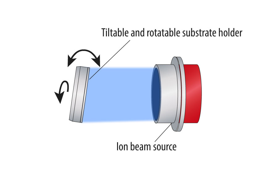
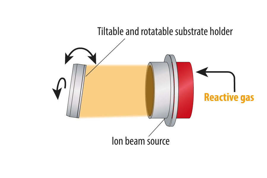
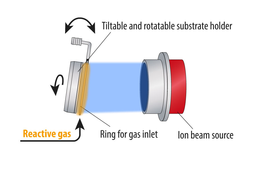
Principle
- Circular ion beam source etches full substrate area under a defined angle with inert or reactive gases
Technologies
Ion Beam Etching (IBE) / Ion Beam Milling (IBM)
uses a collimated beam of inert gas ions for structuring or material removal.
Reactive Ion Beam Etching (RIBE)
introduces reactive gas into the ion beam source for reactive etching of the surface.
Chemically Assisted Ion Beam Etching (CAIBE)
uses reactive gas independent of the ion beam for reactive etching of the surface.
Ion beam Etching (IBE)
Reactive ion beam etching
Chemically Assisted Ion Beam Etching (CAIBE)
Detailed Information
Technical Data
Process Results
Other Ion Beam Etching Systems

scia Mill 200
for full surface etching of wafers up to 200 mm
scia Mill 300
for full surface etching of wafers up to 300 mm

