Ultra-precise Ion Beam Milling of TMR Sensors
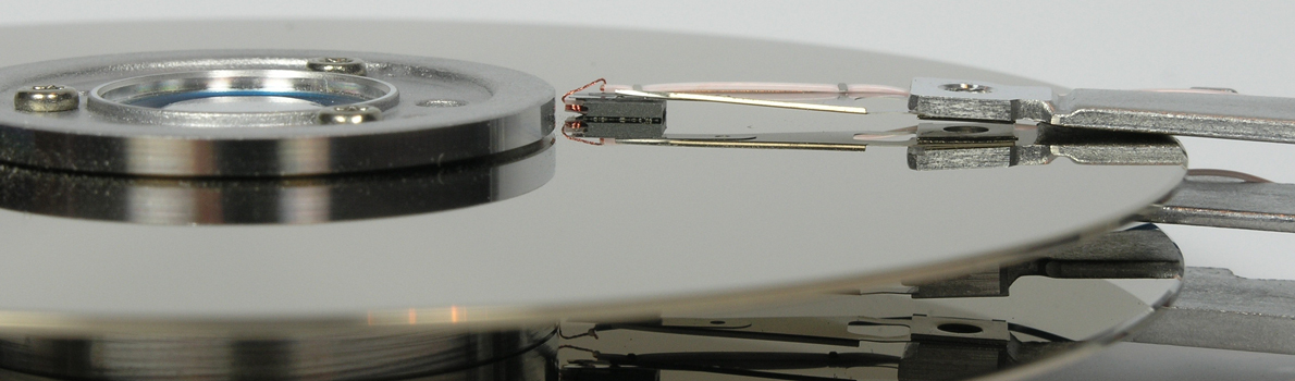
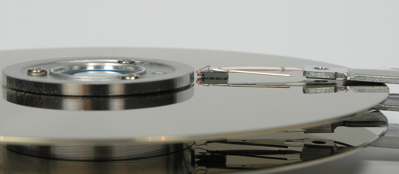
Modern, high-precision sensors use the tunnel magnetoresistance (TMR) effect, which has a wide range of applications, e.g. in the automotive and hard disk drive industries. The main components are magnetic tunnel junctions (MTJs), which exploit the TMR effect. MTJs consist of two ferromagnetic layers separated by a non-magnetic barrier layer.The top layer (free FM layer) changes its magnetization easily by an external magnetic field, while the bottom layer (pinned FM layer) conserves its magnetization until a certain switching field is reached. The electrical resistivity of the MTJ depends on the orientation of the free FM layer compared to the pinned FM layer.
Compared to GMR-based sensors, TMR offers higher thermal stability and an increased signal output with lower power consumption. These advantages have led to rapid market growth.
The production of a TMR sensor requires a complex multilayer structure. During the following etching process for the electrical contacting of the sensor, problems can occur with the usual dry etching process, as magnetic materials such as CoFe, CoPt and NiFe generally have a poor reactivity and the exposed electrodes can corrode due to reactive gases.
Ion beam etching uses argon ions for ion bombardment as an alternative.
...

Fig. 1: Magnetic tunnel junction based on CoFeB/MgO/CoFeB.
Learn more
For more information on ion beam milling for structuring of tunnel-magneto-resistance sensors, please refer to our White Paper.
Reach out
Please contact us for further information.
Related Information
Related Products: scia Mill 150 & scia Mill 200 & scia Mill 300
- Full substrate ion beam milling with superior uniformity
- Etching with inert gases to avoid after-corrosion
- Helium backside cooling contact for substrates allows to use photoresist
- Reactive gas compatibility in RIBE and CAIBE processing
- Ion beam source with high stability, adjustable ion energy and ion current density
- In-situ measurement for exact end point detection with SIMS or OES
- Complete software integration and automated processes via recipe
For additional coating processes the scia Coat 200 is recommended.
