

Substrate size (up to) | 200 mm dia., all standard wafer sizes possible |
Substrate holder | Water-cooled, helium backside cooling contact, electrostatic clamping without edge exclusion |
Axes performance | Max. velocity 0.5 m/s, max. acceleration 15 m/s² |
Ion beam source | 37 mm circular RF source (RF37-i) with 8 ...15 mm (FWHM) or |
Neutralizer | Hot filament neutralizer (N-Fil) or RF plasma bridge neutralizer (N-RF) |
Throughput | 15 Wafer/h (50 nm Si on 150 mm wafer) |
Base pressure | < 1 x 10⁻⁶ mbar |
System dimensions (W x D x H) | 2.80 m x 1.40 m x 2.20 m, for single chamber with cassette handling (without electrical rack and pumps) |
Configurations | Single chamber with single substrate load lock or cassette handling, Cluster system with 2 process chambers and cassette handling |
Software interfaces | SECS II / GEM, OPC |
Precise Surface Correction
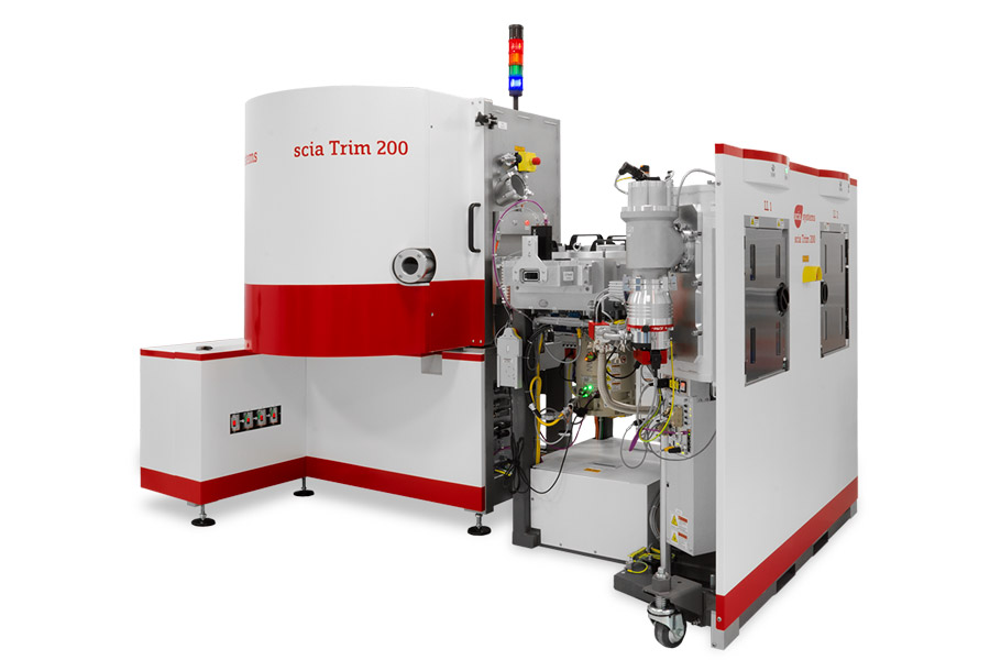
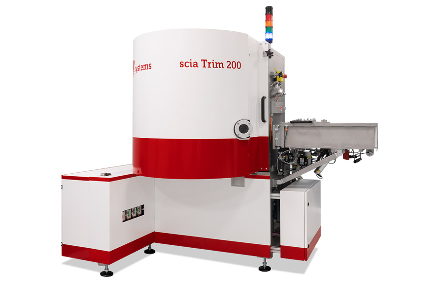
The scia Trim 200 is used for high precision surface trimming of wafers, without limitations in film and wafer materials. Designed for high-volume production the system has a throughput and maintenance optimized layout with a semiconductor cassette handling robot that accommodates all standard wafer sizes. In addition, a cluster configuration with two process chambers and two cassette load locks is available.
Features & Benefits
- Significant yield improvement
- Film thickness homogeneity to be adjusted down to atom level of 0.1 nm
- No edge exclusion with electrostatic chuck
- Sub-nanometer removal with zero base etch function
- Processing of film and wafer materials without restrictions
- Throughput and maintenance optimized design for low production costs
- Processing of wafers with photoresist masks due to good wafer cooling
Applications
Results IBT
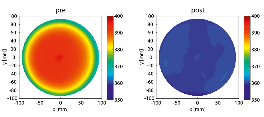
Results (left-pre, right-post) for ion beam trimming of aluminum oxide on a 200 mm wafer. Standard deviation: pre: 9.4 nm, post: 0.4 nm; Improvement factor: 23.5; Average thickness: pre: 382.3 nm, post: 360.1 nm; Target: 360 nm
- Frequency trimming of bulk acoustic wave (BAW) or surface acoustic wave (SAW) filters
- Thickness trimming of silicon on insulator (SOI), quartz, lithium tantalate (LT) or lithium niobate (LN) wafers
- Film thickness error or step height correction in thin film head (TFH) manufacturing
- Dimensional correction of MEMS structures
- Form error correction for X-ray mirrors
Application Notes
- BAW filters as high frequency filters in mobile communication
- SAW-filters for the suppression of frequencies in mobile communications
- Thickness Trimming of POI wafers for RF filters (SAW)
- Film Thickness Correction of read/write heads for hard disks (TFH)
- Surface error correction of X-ray mirrors
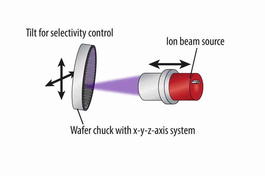
Principle
- Focused broad ion beam scans across wafer surface in vertical setup for low contamination
- Local material removal is controlled by adjusting the dwell time
Technologies
Ion Beam Trimming (IBT) is where a focused broad ion beam scans across the wafer and the local material removal is controlled by adjusting the dwell time.
Reactive Ion Beam Trimming (RIBT) introduces reactive gas into the ion beam source for reactive structuring of the surface.
Ion Beam Figuring (IBF) is a polishing error correction by a scanning ion beam and dwell time control.
Detailed Information
Technical Data
Process Results
Other Ion Beam Etching Systems

scia Trim 300
for large area surface correction of wafers up to 300 mm

scia Mill 200
for full surface etching of wafers up to 200 mm

