

Ion Beam Trimming of POI Wafers for RF Filters
The establishment of new communication standards, such as 5G, requires higher frequencies for mobile data exchange. New SAW (Surface Acoustic Wave) components are used in these frequency ranges, in particular the "guided SAW components" or “Piezo on Insulator” (POI). These components consist of a piezo layer that is bonded to a standard silicon wafer. The structure of the filter components is similar to standard SAW filters, with a piezoelectric substrate, such as quartz, lithium tantalate (LiTaO3), or lithium niobate (LiNbO3), and two sets of interleaved metal electrodes called interdigital transducers (IDTs) on top of the substrate. These structures convert incoming electrical signals into acoustic waves that propagate along the substrate surface and are then transmitted back to the second transducer. Efficient signal transmission only occurs if the signal frequency matches the resonance criteria.
With POI wafers, the acoustic wave is guided within the piezo layer, which enables a higher coupling factor K² and thus filters with a wider bandwidth and high band density, including built-in temperature compensation. POI wafers typically consist of two or three functional layers. In order to keep the surface as flat as possible, the thicknesses of the individual layers must be precisely adjusted. Requirements for layer uniformity and layer accuracy are becoming increasingly demanding. Methods such as grinding and chemical-mechanical polishing (CMP) are often not precise enough. This is where ion beam trimming (IBT) can be used to improve surface uniformity and coating accuracy by removing up to 1 µm of material while maintaining a low surface roughness. The scia Trim 200 enables precise adjustment of the coating thickness through localized ion beam etching.
...

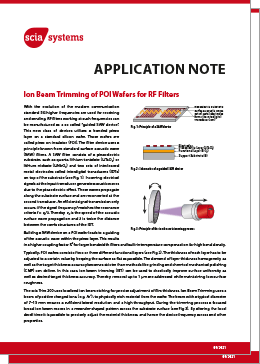
Fig. 1: Principle of a SAW device

Fig. 2: Schematic of a guided SAW device
Reach out
Please contact us for further information.
Learn more
Ion beam trimming of piezoelectric materials
In his video presentation, scia Systems' sales director Marcel Demmler introduces the ion beam trimming process and our process solution scia Trim 200, which can significantly improve the manufacturing yield of piezoelectric devices. He follows up by showing you two application examples including process results.
Related Information
Related Product - scia Trim 200
- System operates all standard wafer sizes from 100 mm to 200 mm dia.
- Film thickness uniformity to 0.1 nm
- Electrostatic chuck for no edge exclusion and low contamination
- Processing of dielectric and metal films
- Significant yield improvement
- High volume production system availabe in cluster layout
Any questions left?
scia Systems GmbH
Clemens-Winkler-Str. 6c
09116 Chemnitz
Germany
