Surface Trimming for Surface Acoustic Wave (SAW) Devices
Modern mobile communication increasingly uses frequency filters since current communication standards are defined with new frequency bands. SAW filters, based on the surface acoustic wave principle, offer remarkable efficiency and suppress frequencies outside the transmission band particularly well, resulting in a high Q factor.
SAW filters consist of a piezoelectric substrate (e.g., quartz, lithium tantalate, or lithium niobate) and interdigital metal electrodes (IDT). Electrical signals at the input transducer generate acoustic waves due to the piezoelectric effect. These waves are transmitted via the substrate to be reconverted at the second transducer. Efficient signal transmission only occurs when the signal frequency matches the resonance criteria.
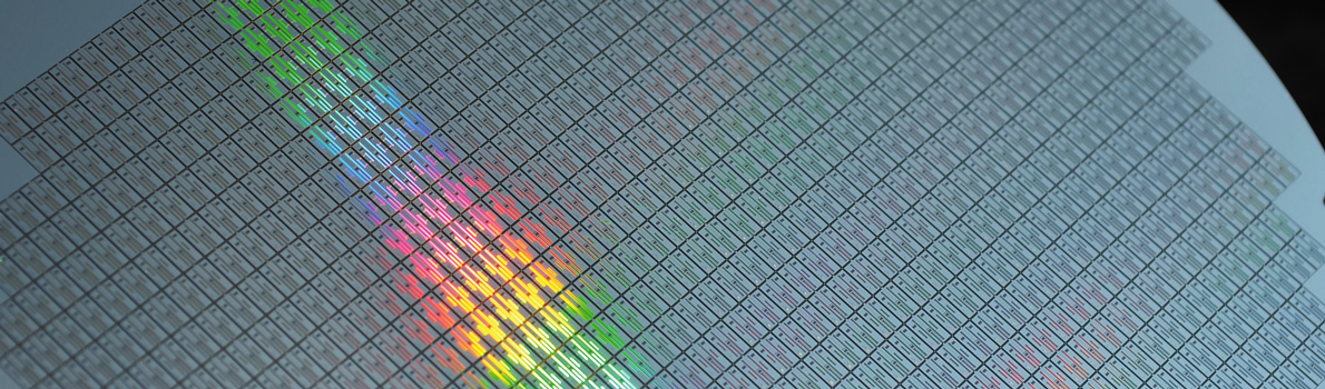
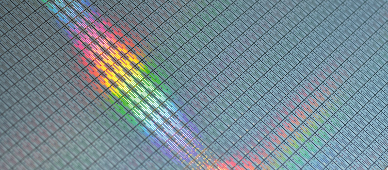
Due to limited frequency bands, carrier aggregation methods are used in 3G and 4G standards in telecommunications to enable parallel transmissions in frequency blocks. To avoid interference, the specifications for bandwidths are becoming increasingly tighter, requiring precise filter manufacturing and SiO2 coatings on the IDTs for temperature drift suppression. Special surface acoustic wave filters with temperature compensation (TC-SAW) additionally use Si3N4 passivation layers to meet the uniformity requirements. However, traditional coating systems show irregularities in both metal coatings for transducers and temperature compensation layers.
Ion beam trimming improves layer uniformity and enables a high component yield in the mass production of (TC) SAW filters.
...

Fig. 1: Basic SAW filter design

Fig. 2: TC-SAW filter layer stack
Reach out
Please contact us for further information.
Learn more
Ion beam technology for thin piezoelectric films
Piezoelectric films are used in a wide range of applications, such as transducers for example in microphones, motors and resonators. The coated resonators are mainly used as frequency filters in modern mobile communications and require an excellent quality of piezoelectric coating. In his presentation, Karl Gündel, Technical Sales Manager at scia Systems, will talk about the advantages of ion beam technology in the production of these piezoelectric layers.
Related Information
Related Product - scia Trim 200
- Thickness trimming, to improve yield
- Increase in device yields to over 90 %
- High volume production system
- Equipped with handling robot for standard semiconductor cassettes
Any questions left?
scia Systems GmbH
Clemens-Winkler-Str. 6c
09116 Chemnitz
Germany
