Sputter Deposition of Silicon Dioxide for Temperature Compensation of SAW Filters
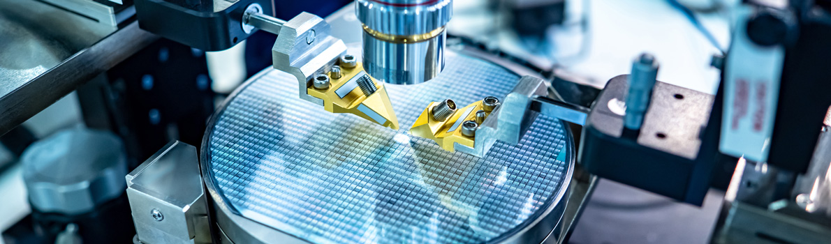
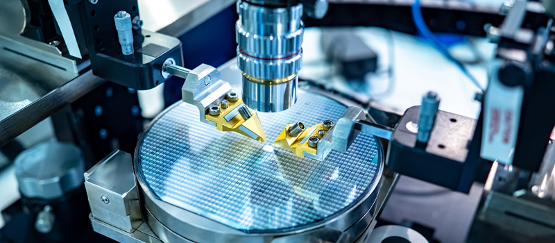
Temperature compensated surface acoustic wave (TC-SAW) frequency filters have opened a new field of applications in mobile communication. As standard SAW filters show a temperature-dependent frequency drift of -20 ppm/K up to -40 ppm/K, many high-frequency applications as well as communication in narrow RF bands would not be possible. The application of silicon dioxide (SiO2) for temperature compensation (see Fig. 1) allows the reduction of the temperature-dependent filter frequency drift (TCF) of a TC-SAW filter down to 0 ppm/K. However, the filter performance strongly depends on the quality of the deposited SiO2 as it contributes to the acoustic wave propagation. Especially, a dense and closed layer growth on the interdigital transducer (IDT) is challenging due to the high aspect ratio and varying seed material. In parallel, the industry requirement of high wafer throughput has to be fulfilled.
The required SiO2 for TC-SAW filter can be deposited using a scia Magna 200 reactive sputter deposition system. Magnetron sputtering from a silicon target in an argon/oxygen gas mixture allows the stoichiometric deposition of SiO2 with a high deposition rate. The use of a RF substrate bias significantly influences the layer growth on the SAW IDT structures.
...
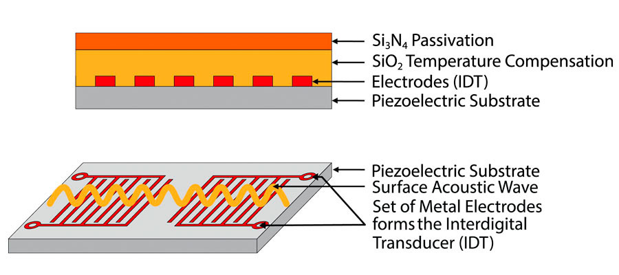
Fig. 1: Schematic view of a typical TC-SAW stack and functional principle.
Acknowledgment: The research has been funded by the European Union and the Free State of Saxony. Funding reference: 100206216/10020621618.
Reach out
Please contact us for further information.
Related Information
Related Product - scia Magna 200
- Cluster configuration with automated wafer handling, cassette loading
- Recording of process data, production log and component lifetime counter
- Easy standard maintenance e.g. target and sputter shield exchange
- Fab interface possible (e.g. SECS II/GEM)
