Ion Beam Etching for Reverse Engineering
Reverse engineering (RE) is an essential step in the production of integrated circuits (IC) based on wafers. It aims to verify existing structures, analyze defects and expose them for research purposes. The RE process comprises four main steps:
- decapsulation, to expose internal components of the chip to examine dies, interconnections, and other features
- delayering including a destructive layer-by-layer analysis of the die to see each metal layer, passivation layer, polysilicon layer, and active layer
- imaging, typically realized by SEM, TEM or SCM
- postprocessing with functional analysis and identification of chip
The ongoing development of chips with higher power density places high demands on more precise layer removal methods. Conventional processes such as wet chemical etching, chemical-mechanical polishing (CMP) or plasma etching are often expensive, error-prone and limited in application for modern chips. Ion beam etching offers a solution, as it enables precise processing within the µm and nm size range and atomic level thickness range for different materials at once. The process involves active ion bombardment of the substrate with reactive and inert gas ions to chemically and physically etch the material from the surface.
...
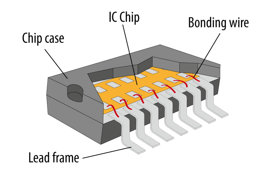
Fig. 1: Schematic view of an integrated circuit (IC) chip device
Reach out
Please contact us for further information.
Related Information
Related Products: scia Mill 150 & scia Mill 200 & scia Mill 300
- Etching with inert gases to avoid after-corrosion
- Helium backside cooling contact of substrates for use of photoresist
- Reactive gas compatibility in RIBE and CAIBE processing
- Ion beam source with high stability, adjustable ion energy and ion current density
- In-situ measurement for exact end point detection with SIMS or OES
- Complete software integration and automated processes via recipe
