Magnetron Sputtering of Silicon Dioxide
Silicon dioxide (SiO2) is an important material for manufacturing of semiconductors and microelectromechanical systems (MEMS). It is mainly used for passivation or insulation films and as dielectric layer.
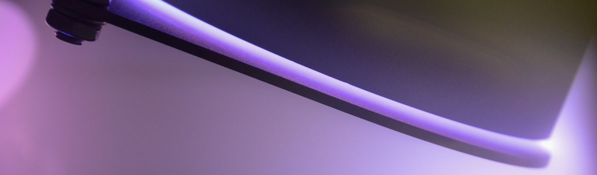
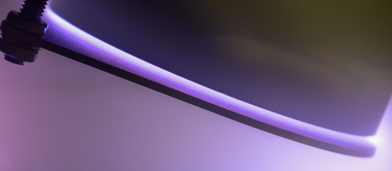
One application example is the deposition of SiO2 as temperature compensation layer for TC-SAW filter devices in mobile communication. The performance of those filters strongly depends on the quality of the deposited SiO2 layer. Therefore, a cost-effective solution for high volume production with reliable process results and high wafer throughput is needed.
Advantages of magnetron sputtering for silicon dioxide deposition
- Dense films with high homogeneity and good purity
- Excellent coating precision
- Deposition with high rates
- Low substrate temperature allows processing of materials that are very fragile and sensitive to high temperatures and rapid temperature changes
- Variation of film properties by adjustable energetic substrate bombardment
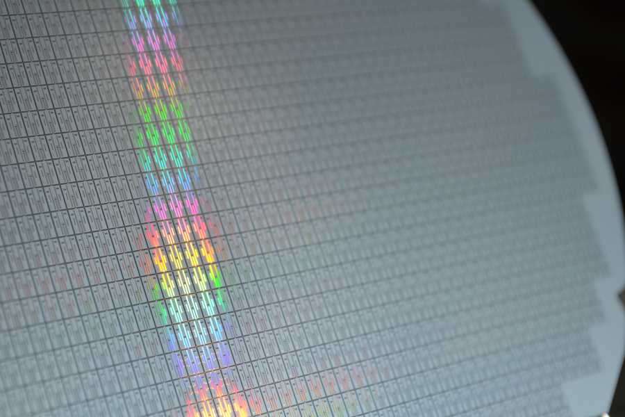
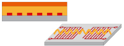
Wafer with SAW filter components
Technology
Learn more about magnetron sputtering and the different possible sputter setups in our technology overview.
Application
In our Application Note we show you, how sputter deposition of SiO2 is used for the temperature compensation of SAW filter devices.
Product
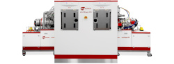
The scia Magna 200 is a coating system that is made for precise deposition of metals and/or dielectric layers on wafers up to 200 mm.
Do you want to speak to one of our experts? Contact us:
scia Systems GmbH
Clemens-Winkler-Str. 6c
09116 Chemnitz
Germany
Tel: +49 371 33561-0
✉ sales@scia-systems.com
Additional Information
Overview of PVD Technologies
Comparison of ion beam sputtering, magnetron sputtering and evaporation.
Ion beam trimming of POI wafers
Video presentation: Surface correction of piezoelectric materials