
Mobile Communication: How Ion Beam Technology Produces High-Quality Frequency Filters
In every cell phone are components that have been manufactured on the production lines of scia Systems. But what is our specific contribution to mobile communications?
1G, 2G/GSM/EDGE, 3G/UMTS/HSDPA, 4G/LTE or 5G - no matter how confusing the variety of terms in the mobile communications world might be, the basic principle is always the same: The signals are modulated onto a carrier frequency. In addition to the frequency, the used transmission protocol determines the available data rate to a large extent. Both, mobile devices and base stations, must adhere precisely to these carrier frequencies. Today, these carrier frequencies range in Europe from 890 MHz to 3.8 GHz, depending on the used mobile communication standard.

Extract of the spectrum of electromagnetic waves
The carrier frequency is defined for both mobile devices and base stations by precisely tuned frequency filters. In mobile communications, the transmit and receive channels are also on adjacent frequencies to enable simultaneous listening and speaking.
The filters are not built from coils and capacitors (LC networks) as usual in electrical engineering. The clever idea is to use an acoustic wave instead of filtering the electromagnetic wave.
According to λ=v0 / f the wavelength scales with the propagation speed of the acoustic wave for a given frequency. Compared to a propagation with nearly speed of light for the electromagnetic wave, the velocity of propagation of an acoustic wave in quartz is 6,000 m/s, which is 50,000 times slower and leads to 3 µm wavelength at 2 GHz. Therefore, it is possible to build miniaturized electro-acoustic filter components with suitable geometric structures in the µm range. In addition to the filter effect, parameters such as insertion loss or Q-factor play an important role, but they are not discussed further here.
Step 1: SAW
The principle of filtering acoustic waves was established in the 1950s in so-called surface acoustic wave (SAW) filters. A comb-shaped structure consisting of two electrodes is applied to a solid piezoelectric wafer (today mostly made of lithium tantalate LiTaO3 or lithium niobate LiNbO3). The desired signal is applied to these electrodes, which excites a surface acoustic wave on the piezoelectric material with a λ/2 wavelength corresponding to the electrode spacing. A second electrode structure with the same geometry converts the acoustic wave back into an electrical signal. The distance between the electrodes determines the geometric resonance conditions, so that only the frequency corresponding to λ/2 is transmitted.

Surface acoustic wave (SAW) filter with comb-shaped electrodes for producing and reconverting of the acoustic wave.
This simple design enables the production of low-cost SAW filter elements. However, there are three significant disadvantages:
- Temperature shifts due to the expansion of the piezoelectric base material cause a change in the electrode geometry and thus a frequency drift.
- The oscillation energy is not exclusively directed into the surface wave; part of it is lost in the bulk material.
- The electrode spacing, which cannot be reduced infinitely, limits the accuracy. Therefore, SAW devices are only used at long wavelengths in the lower frequency range.
Step 2: TC-SAW
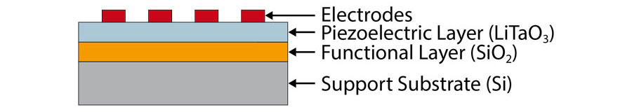
The first step to overcome the disadvantages were Temperature compensated SAW (TC-SAW). A temperature compensation layer (usually high density SiO2) with an alternating temperature drift compared to the wafer material is deposited on the front side of the substrate. In addition, a passivation layer (Si3N4) is applied to achieve a significant improvement in thermal stability.

Cross-section of a temperature-compensated surface acoustic wave (TC-SAW) filter. The SiO2 layer has alternating thermal properties to the substrate.
Step 3: Guided SAW
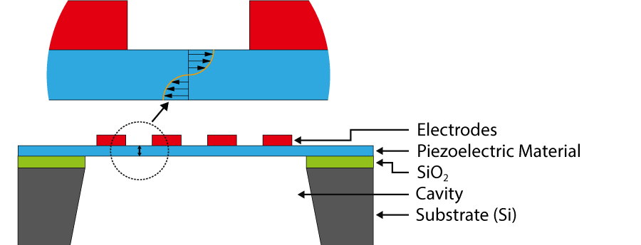
Guided SAW devices have been manufactured for a few years now as a consistent further development. In these new types of SAW components, only a thin piezoelectric layer is used on a carrier wafer. Two wafer materials, usually silicon as base and LiTaO3 or LiNbO3 as the functional material, are bonded together for this purpose. The piezoelectric material is then reduced to the desired thickness by milling and polishing. The bonded material ensures an intrinsic temperature compensation and at the same time the energy of the surface wave remains exclusively in the bonded material. The waveguide function can be supported even further via additional intermediate layers.
Cross-section of a guided surface acoustic wave (SAW) filter. The surface wave propagates only in the LiTaO3
Step 4: BAW
As mentioned earlier, SAW devices are used primarily at long wavelengths and thus in the lower frequency range of mobile communication.
Volume resonators (Bulk Acoustic Wave, BAW) cover the necessary precision in the higher frequency range. BAW devices are manufactured using thin-film technology, in which a piezoelectric material (scandium-doped aluminum nitride/Al(Sc)N) is excited between two electrodes (molybdenum or tungsten) to produce volume oscillations. Resonance occurs, if the half wavelength of the acoustic wave corresponds exactly to the layer thickness of the stack.
Resonance frequencies can be set very precisely with the layer thickness. The only requirement is that the resonator is decoupled from the silicon substrate. Two methods are used for this acoustic decoupling: In the FBAR (Free Bulk Acoustic Resonator) type, by release etching a cavity is built under the component so that the resonator remains cantilevered on the substrate. In the SMR (Solidly Mounted Resonator) type, an acoustic mirror is deposited underneath the resonator. This mirror, consisting of alternating high- and low-refractive-index materials, reflects the acoustic wave back into the piezoelectric material.
Even though they have obvious technical advantages over SAW devices, the manufacturing steps of BAW filters are significantly more complex and therefore more expensive, which is why they are used exclusively in the upper frequency range.
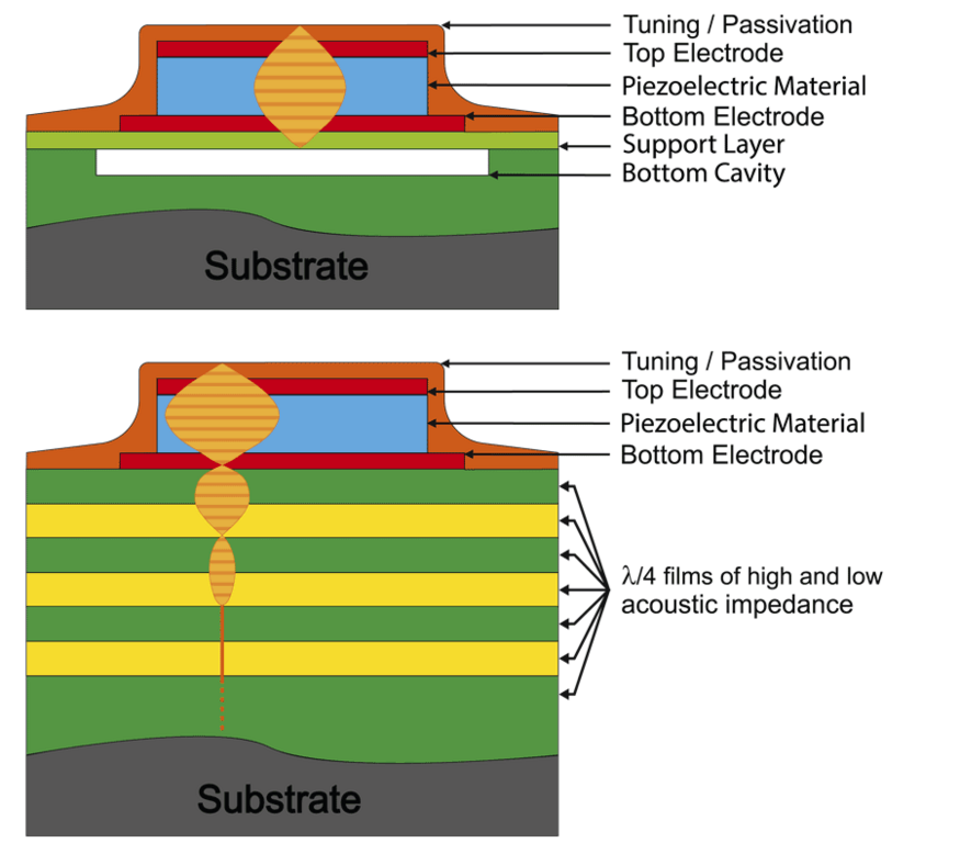
TOP: FBAR-BAW resonator with freely etched cavity. BOTTOM: SMR-BAW resonator with acoustic mirror for acoustic isolation.
Step 5: XBAR
Nowadays further developments in devices no longer establish completely new functional principles, but rather optimize existing solutions. One example are XBAR components, which are currently under development. Basically, the principle corresponds to a freely etched, guided SAW on the back. Technically, the fabrication is not a huge challenge either. Due to the lack of backside support, shear vibrations are now excited in the arrangement. Using this principle, it is now possible to filter frequencies in higher and higher GHz ranges.
Basic arrangement of an XBAR and schematic representation of excited shear waves.
How does scia Systems contribute to the development and production of these filter components?
scia Systems develops process technologies and has contributed some pioneering ideas to the implementation of technological ideas in equipment. Primarily, of course, we equip the manufacturers of filter elements with our systems. Thereby we serve the following process steps:
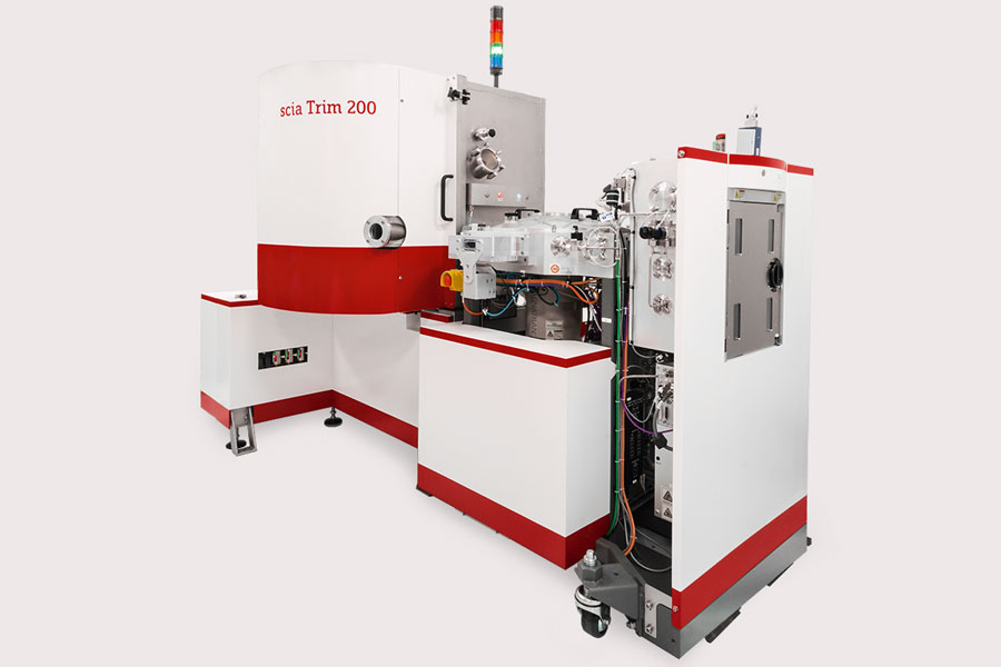
scia Trim 200
The systems are used to correct geometric deviations spread over the wafer, which, if uncorrected, would result in frequency variations and thus significant yield losses. Therefore, the processes established on the scia Trim 200 are always used by filter manufacturers worldwide for local frequency correction for:
- Trimming the temperature compensation of TC-SAW: The transmission frequency can be precisely adjusted via layer thickness trimming of the temperature compensation layer.
- Trimming the layer thicknesses of FBAR and SMR: First of all, the layer thickness of the Al(Sc)N resonator has to be aligned to the target frequency. Furthermore, the acoustic mirror of SMR and the passivation of both BAW types need also to be trimmed.
- Trimming of compound wafers: Mechanical processing steps for thinning the deposited piezoelectric wafer are not accurate enough and require local correction of the remaining material thickness.
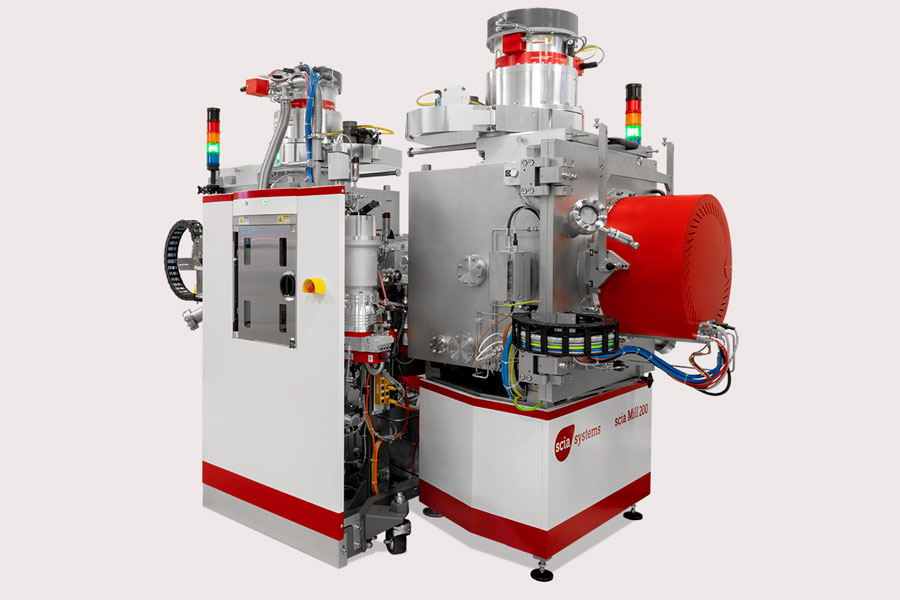
scia Mill 200
With this ion beam etching system, a constant material removal can be performed over the entire wafer. Thus, structuring steps can be carried out for many filter manufacturers, such as:
- Frequency shift across the entire wafer: A consistent frequency shift can be performed faster and more effectively using the scia Mill 200 than the scia Trim 200. With a masked transmit channel, the receive channel can be shifted to the desired higher frequency by material removal.
- Structuring of electrodes. Multilayer electrodes used at higher frequency can be structures by ion beam milling.
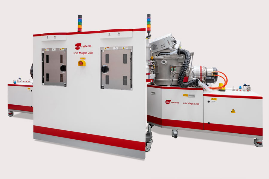
scia Magna 200
This magnetron sputter system is used for the deposition of functional coatings. It can also be used for the following processes:
- Deposition of AlN or Al(Sc)N: The processes are always done reactively with Al- or scandium-doped Al target and a reactive gas.
- Deposition of temperature compensation of TC-SAW: SiO2 layers with high density can be deposited reactively with high RF bias voltage. Currently fluorine-doped SiO2, which can be used to realize full temperature compensation, is gaining more interest in TC-SAW manufacturing.
Any Questions left?
Do you want to speak to one of our experts? Contact us, our team will be happy to help you.
scia Systems GmbH
Clemens-Winkler-Str. 6c
09116 Chemnitz
Germany
Additional Information
Application Notes
Selected applications for MEMS, optics and sensors, presented in detail.

Ion beam for piezoelectrics
Video presentation: Benefits of ion beam technology for piezoelectric films