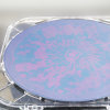
Video presentation: Direct etching of slanted gratings for waveguides

In this video presentation, Sales Director Marcel Demmler will introduce the latest results for etching of slanted relief grating (SRG) used as in- and out-coupling gratings in waveguides for augmented or mixed reality devices.
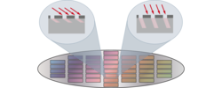
The smaller input grating diffracts light coming from a display into the waveguide. At the out-coupler grating, light is diffracted in direction of the viewer. The geometrical dimension of the gratings has to be smaller than the wavelength of the light. Different approaches for the design of coupling gratings exist. One type is the so called SRG, which has a higher coupling efficiency compared to other types. For SRG, tilted trenches are etched in the waveguide, which is typically a plate made of a high refractive index material.
The manufacturing challenges are the control of etching depth, slant angle and bottom angle. Marcel Demmler will introduce a reactive ion beam milling tool for manufacturing of those gratings in mass production. He concludes by showing examples of how process parameters can be varied in order to control the grating geometry.
Here you can see the presentation.
Technology
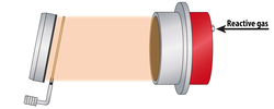
Learn more about Reactive Ion Beam Etching (RIBE) and Chemically Assisted Ion Beam Etching (CAIBE) in our technology overview.
Application
In our Application Note, we show you how to use Reactive Ion Beam Etching to process surface relief gratings for AR- & MR-devices.
Products
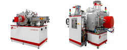
The scia Mill 150 and scia Mill 200 are both systems with reactive gas compatibility in RIBE and CAIBE processing, including fluorine/chlorine gases.
Do you want to speak to one of our experts? Contact us:
Additional Information

Ion beam figuring for telescope mirrors
Video presentation: surface error correction in high vacuum

Ion beam etching for optics structuring
Video presentation: How to structure your optics with reactive ion beam etching.