Video presentation: Processing of optical gratings with varying slant angles by reactive ion beam trimming

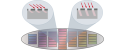
Augmented and mixed reality devices have gained a lot of interest in the last few years. At the center of this technology are lightweight, close-to-eye displays. To create these displays, you need surfaces with relief gratings, which are used to couple light from the source into the waveguide and out of it towards the eye. The gratings are slanted to suppress higher diffraction orders and thus maximize the light output.
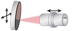
To realize a wide field of view it is highly desirable to have a variation of the slant angles. However, this is difficult to achieve using nanoimprint lithography, i.e. filling the grating material into a mold and then curing it. The grating could break due to the opposite directions of the trenches, when it is lifted off. Therefore, the solution is: ion beam trimming, a special form of ion beam etching that uses a focused ion beam to scan across the substrate.
Ion Beam Trimming (IBT) is a well-established method in the MEMS industry to locally change the thickness of a functional layer on a substrate. This method was adapted for the production of surface relief gratings with varying slant angles and varying trench depth. The dwell time of the ion beam defines the trench depth and the angle of incidence determines the angle of inclination of the individual trenches. Both parameters can be varied locally and independently of each other.
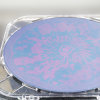
In the video, Dr. Carsten Schulze introduces our ion beam etching system scia Trim 200 and shows the results of processing SiO2 wafers with chromium mask.
In conclusion he reveals that ion beam trimming offers a very flexible approach to the production of slanted surface gratings, whether for single wafers or for high-volume production.
Here you can see the presentation.
Technology
Learn more about ion beam trimming and other ion beam processes in our technology overview.
Application
In our Application Note, we show you how to use Reactive Ion Beam Etching to process surface relief gratings for AR- & MR-devices.
Product
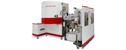
The scia Trim 200 is used for high precision surface trimming of wafers up to 200 mm, without limitations in film and wafer materials.
Do you want to speak to one of our experts? Contact us:
scia Systems GmbH
Clemens-Winkler-Str. 6c
09116 Chemnitz
Germany
Tel: +49 371 33561-561
✉ sales@scia-systems.com
Additional Information
Ion beam figuring for telescope mirrors
Video presentation: surface error correction in high vacuum

Gratings with constant or variable slant angle
Video presentation: Advanced Patterning for Surface Relief Gratings