

Patterning of Lithium Niobate via Ion Beam Etching for Photonic Integrated Circuits (PICs)
Photonic Integrated Circuits (PICs) are a breakthrough technology that combines the advantages of photonics with the efficiency of integrated circuit technology. These circuits enable the manipulation of light on a chip, leading to a wide range of applications in telecommunications, sensing, computing, and many other fields.
PICs consist of various optical components. These include light sources, modulators, detectors, and waveguides. Those components work together to generate, control, and receive light signals. Among the materials used for PICs, Lithium Niobate is particularly promising for optical waveguides and modulators. Its strong Pockels effect, with an electro-optic coefficient of approximately 30 pm/V, enables efficient modulation of light by applying an electric field.
This application note demonstrates ion beam etching for pattern transfer in fabricating lithium niobate (LiNbO3, abbr. LN) waveguides.
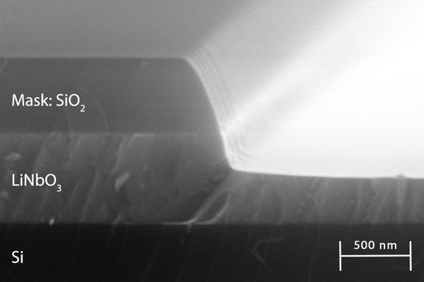
SEM micrograph of ion-beam-etched LiNbO3 waveguides

Reach out
Please contact us for further information.
Learn more
Enhancing PIC Production with Ion Beam Technology
scia Systems' advanced ion beam etching and trimming processes optimize the patterning and uniformity of microstructures for photonic integrated circuits (PICs)
Related Information
Related Product - scia Mill 200
- Full surface etching with superior uniformity
- Reactive gas compatibility in RIBE and CAIBE processing, including fluorine / chlorine gases
- Substrate holder featuring rotation and tilt for arbitrary angles of incidence
- Thermal control of wafers during the process over a wide temperature range
- Ion beam source with high stability, adjustable ion energy and ion current density
- Complete software integration and automated processes via recipe
Any questions left?
scia Systems GmbH
Clemens-Winkler-Str. 6c
09116 Chemnitz
Germany