

Precise Chip Delayering for Failure Analysis & Material Inspection
Sequential layer-by-layer removal of ICs with sub-nanometer precision across common materials, without structural damage, for wafers up to 300 mm.
What is chip delayering?
Chip delayering is the controlled, sequential removal of layers in a multi-layer integrated circuit to reveal individual layers for visual or analytical inspection. It is a core step in both failure analysis and material inspection workflows.

Typical layer stack of an IC chip
Who uses chip delayering?
Physical Failure Analysis
- Used by semiconductor manufacturers, test labs and Research and development
- Identify root causes of device failures, defects in interconnects, or process-induced damage.
- Uncover opportunities for optimization and cost factors
- Find security weaknesses
Law Enforcement
- Layer-by-layer removal of materials, used by law enforcement, government agencies, and authorized security research teams.
- Reconstruct netlists, identify materials and architectures for criminal investigation
- Find access to read out data from integrated circuits (e. g. mobile phones)
- Verify authenticity, detect tampering
Competitive Intelligence
- Delayering used by semiconductor industry
- Analyze competitor devices to understand architecture and material choices
- Gain transparency into the chip's construction
- Supports product benchmarking and technology roadmapping
Why ion beam etching for delayering?
Well-established techniques such as mechanical preparation, wet chemical etching, dry plasma etching and focused ion beam (FIB) processing all have fundamental trade-offs. IBE achieves greater precision than mechanical prep and faster results than FIB.
Advantages of ion beam etching:
- IBE is a kinetic process
- Suitable for a wide range of materials, including metals, semiconductors, polymers, and ceramics
- No dependency on chemical reactions
- Low temperature (<100 °C)
- to minimize thermal deformation or damage to the material
- to minimize thermal deformation or damage to the material
- High precision delayering down to atomic-level thickness range
- Dimensional accuracy due to anisotropic etching
- Precise control of etch rate
- Precise endpoint detection
- Adjustable angle of incidence
- Adjustable material selectivity

How ion beam delayering works

Ion beam generation & gas tuning
A broad ion beam is directed at the wafer surface in a vacuum chamber (~10-4 mbar). The mixture of inert and reactive ions, angle, and energy controls the material selectivity while achieving highly uniform etching.

Thermal & structural protection
Helium backside cooling keeps substrate temperature low, while precise beam control preserves device integrity. No mechanical stress, no ion implantation damage.

Real-time endpoint detection
OES (Optical Emission Spectroscopy) or SIMS (Secondary Ion Mass Spectrometry) monitors material removal continuously, enabling precise etch stops before, within, or after any individual layer down to sub-nm films.

Ion beam milling uses a broad beam of positive charged ions, e.g. Ar+, to physically etch material from the wafer substrate by ion bombardment.

Signal intensity in SIMS or OES creates trend lines for each material.
Equipment for ion beam etching
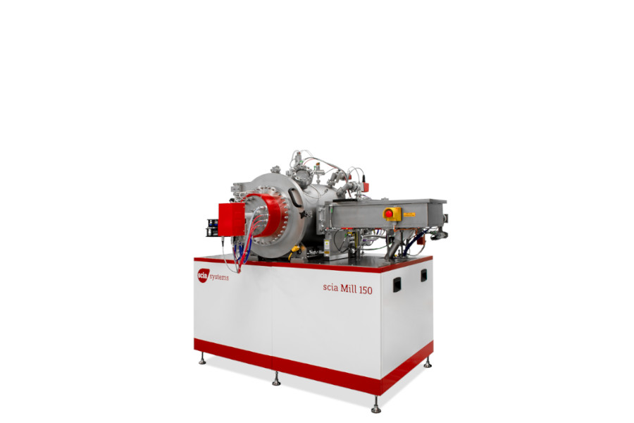
System for small scale production and R&D applications of substrates up to 150 mm
- Ion Beam Etching
- Reactive Ion Beam Etching
- Chemically Assisted Ion Beam Etching
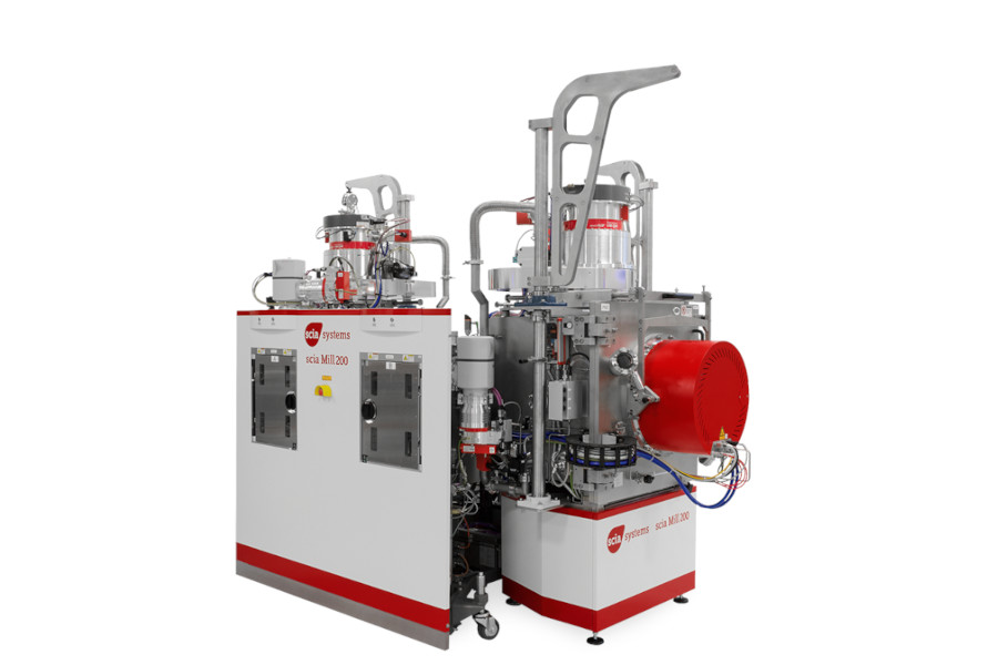
Fully production proven system for mass production of wafers up to 200 mm
- Ion Beam Etching
- Reactive Ion Beam Etching
- Chemically Assisted Ion Beam Etching
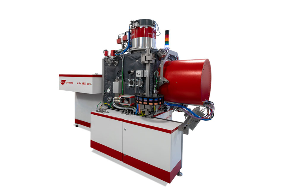
Full surface etching system for wafers up to 300 mm
- Ion Beam Etching
- Reactive Ion Beam Etching
- Chemically Assisted Ion Beam Etching
Learn more
Application Note: Ion Beam Etching for Chip Failure Analysis and Material Inspection
Failure Analysis and Material Inspection are essential steps in the production of wafer-based integrated circuits (ICs). It aims to verify existing structures, analyze defects and expose them for research purposes.
In our application note, we demonstrate a typical delayering procedure using a scia Mill 200 with OES detection.

Ion Beam and Plasma Technology for MEMS Production
Our technologies for thin film coating, dry etching and precision cleaning are essential for applications in smart sensors, high-frequency electronics, power electronics and advanced electronics packaging.
Technologies featured in the video:
- Improving RF-filter production by frequency trimming with scia Trim 200
- Ion beam processing of waveguides for Photonic Integrated Circuits (PIC)
- Structuring of micro-optics
- Failure analysis with precise layer-by-layer material removal
- Enhancing sensor technology with increased sensitivity & energy efficiency
- Structuring of TMR Sensors via ion beam etching
Ask for your dedicated solution!
scia Systems GmbH
Clemens-Winkler-Str. 6c
09116 Chemnitz
Germany
Tel: +49 371 33561-0