
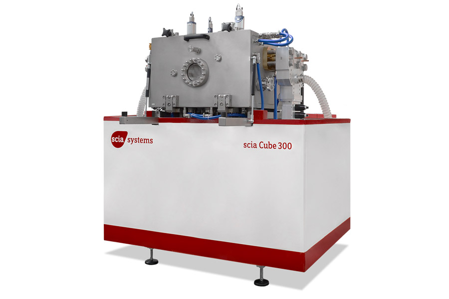
Substrate size (up to) | 300 mm x 200 mm |
Substrate holder | Water-cooled, RF bias |
Substrate temperature | Alternatively cryo-cooling down to -10 °C or heating up to 850 °C |
Plasma sources | 2 linear microwave sources (PL400) and/or |
Power supply | MW power: max. 9 kW, RF power: max. 0.6 kW |
Base pressure | < 1 x 10⁻⁶ mbar |
System dimension (W x D x H) | 1.30 m x 1.90 m x 1.50 m (without electrical rack and pumps) |
Configurations | Single chamber, optional single substrate load lock |
Software interfaces | SECS II / GEM, OPC |
Large Area Coating and Etching over 300 mm x 200 mm
The scia Cube 300 is designed for large area high-density plasma processes. The system enables deposition with high rates and a wide range of deposition parameters. In addition, etching processes with oxygen or halogen chemistry for high anisotropic etching and/or optimized selectivity are possible.
Features & Benefits
- Large area processing with an array of synchronized linear microwave sources
- Independent RF bias at substrate holder for energetic substrate bombardment
- Substrate cooling (-10 °C) or heating (850 °C)
- In-situ chamber cleaning process
Applications
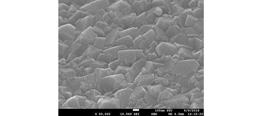
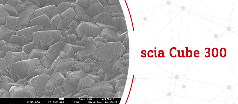
SEM image of grown synthesized boron doped diamond (BDD) layers with courtesy of STU Bratislava . Processing at very low temperature (390 °C). Growth rate of high-quality BDD up to 70 nm/h.
- PECVD Processes
- Deposition of dielectric films, e.g. encapsulation, barrier coatings, electric insulation (SiO2, Si3N4, …)
- Optical and scratch resistant coatings (a-C:H, DLC)
- Growing of nano-crystalline diamond and carbon nanotubes
- RIE Processes
- Reactive etching and structuring of metals (Ni, Cr, Pt, …)
- Etching of gratings and other structures in optical materials (quartz, fused silica)
- Ashing of photoresist
Application Note
- Deposition of DLC for glass compression molds
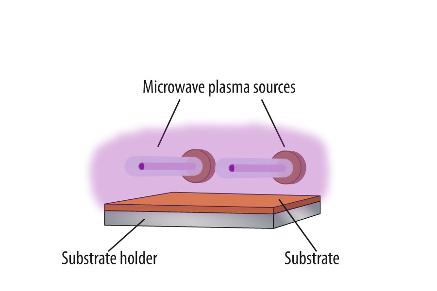
Principle
- Plasma of reactive gases is created by microwave sources
- Enhanced ion bombardment with RF bias
Technologies
Plasma Enhanced Chemical Vapor Deposition (PECVD) is a plasma assisted reactive process to deposit thin films from a gas state (vapor) into a solid state on a substrate.
Reactive Ion Etching (RIE) uses reactive gases and ion bombardment for physically and chemically etching of the substrate surface.
Detailled Information
Technical Data
Process Results
More PECVD/RIE Systems

scia Batch 350
for 3D - coatings in batches

