
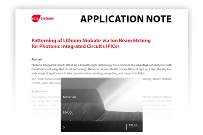
Patterning of Lithium Niobate via Ion Beam Etching for Photonic Integrated Circuits
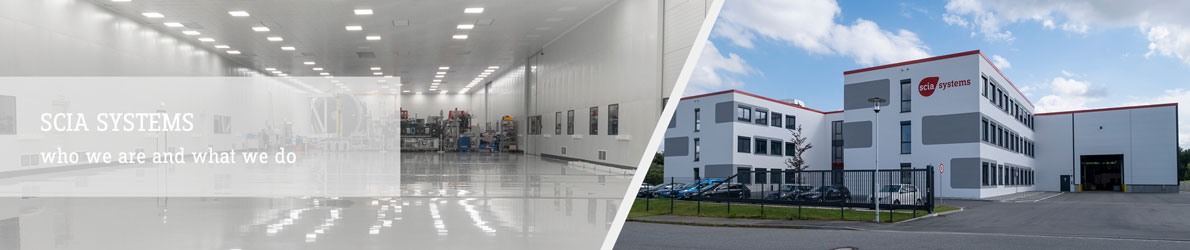
The company was founded 2013 in partnership with the VON ARDENNE GmbH from Dresden and is located in Chemnitz, Germany. As manufacturer of precise surface processing equipment, based on advanced ion beam and plasma technologies, scia Systems established itself in a very short time on the worldwide market. Our customers are companies and research institutes, mainly in the field of microelectronics, MEMS and precision optics manufacturing.
scia Systems stands for highly reliable equipment to meet expectations for today and the future. To ensure our high standards, we work closely with our customers to optimize tool performance and meet the future roadmap requirements. To ensure an optimum and individual customer support scia Systems built up a worldwide network of local sales and service partners.

Managing Directors (f.l.t.r.): Robert Rückriem, Dr. Michael Zeuner and Dr. Michael Gempe

System Design
New design or adaption of standard systems in design and/or process

Manufacturing
In-house manufacturing of core components and integration of high-quality standard components

Software Development
Complete in-house software development and worldwide remote access support

Research & Development
Own department for process optimization and support

Installation & Training
Worldwide Commissioning, on-site assembly & customer training

Service & Support
Maintenance, spare parts and retrofits



EFDS
European Society of Thin Films

SEMI
Industry Association for Semiconductor Equipment and Materials International

SEMI FOA
Fab Owners Alliance

SAWLab Saxony
The scientific network for acoustoelectronics!

SPIE
International society for optics and photonics.

Inplas
Network of Competence of Industrial Plasma Surface Technology

We are certified according to EN ISO 9001:2015.