Raytron Research Institute expands its technology with a system for localized ion beam etching: the scia Trim 200
A new scia Trim 200 system was commissioned by recently founded Yantai Qixin Semiconductor Technology Institute Co., a company jointly invested by Raytron Technology Co. and Yantai local government.
The Chinese high-tech company Raytron is famous for its infrared imaging and MEMS sensor devices. It provides customers with uncooled thermal imaging MEMS sensors, thermal imaging detectors, ASIC chips (Application-Specific Integrated Circuit), thermal imaging and temperature measurement modules, thermal cameras, laser products and optoelectronic systems.
Driven by the corporate vision to become the most valuable chip company in China, Raytron invested in a new company, Yantai Qixin Semiconductor Technology Institute Co. which is now enhancing its technology with an ion beam trimming system. Raytron Research Institute, where the scia Trim 200 will be located, will be built as an open platform, meaning local universities and enterprises can also use this infrastructure and the equipment.
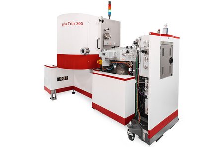
The scia Trim 200 will be used for surface error corrections on substrates up to 200 mm. By feeding the system with the wafer-specific exact thickness distribution, the dwell time of the ion beam can be calculated, which controls the local material removal. In this way, non-uniformities of the deposited layers are improved until an impressively smooth film is achieved.
The scia Trim 200 is a high-volume production system and will not only be dedicated to produce BAW-filters, Yantai Qixin Semiconductor Technology Institute also plans to use the tool for phase array acoustics devices.
We are very happy about this successful cooperation and we are already looking forward to many exciting research results.
- More information about the system and the possible applications you will find here: scia Trim 200.
- Learn more about the technology of ion beam trimming.
- Any questions left? Our team will be happy to help you. Contact us!
