
Dual Ion Beam Deposition of Nano Anti-Wear Coatings for Precision Micro Cutting Tools
The miniaturization of components is an unbroken trend in many industrial sectors, such as medical technology, automotive engineering, aerospace, tool and mold manufacturing as well as microelectronics. A major cost factor in the production of these components is the limited lifespan of the tools due to high wear. Standard coating processes such as CVD (chemical vapor deposition) and PVD (physical vapor deposition) can extend the service life. However, these coating processes produce layer thicknesses in the µm range, which result in rounded cutting edges that lead to significant quality deficiencies for sub-mm drill diameters.
New coating solutions are required to produce layers that meet the following requirements:
- Very small coating thickness to avoid rounding of the cutting edges
- Uniform layer thickness, especially along the cutting edges
- High coating thickness uniformity over a large number of tools
- Hard coatings for low wear
- Good adhesion to the tools, because premature chipping of the coatings would significantly shorten the lifetime of the tools compared to uniform abrasion caused by wear
- Heat resistance, as high cutting speeds lead to significantheating of the tool material
- Cost-effective, so that the coatings are as economical as possible
As part of the “NanoTools” joint project, it has been demonstrated that both atomic layer deposition (ALD) and dual ion beam deposition (DIBD) are capable of producing thin coatings that lead to an increase in service life of up to 6 times by investigating Al2O3 coatings on commercial drills with diameters of 3 mm and 0.3 mm. (see also news of 2017-06-02)
Based on these results, the aim of the follow-up project ENAL (Einsatz Nanobeschichteter Werkzeuge in der Leiterplattenfertigung - Use of Nanocoated Tools in PCB Manufacturing) was to carry out extensive, near-production tests on micro tools to develop a new generation of coated micro cutting tools with nano wear protection coatings, thus reducing the manufacturing costs of various cutting tools used for fine or micro machining.
Since ALD proved to be uneconomical due to the long coating time, ENAL focused exclusively on coatings with DIBD. However, for very small drills with drill diameters of less than 0.5 mm, SEM images showed spalling along the cutting edge after only a short period of use. The main reason for the differences to drills with a diameter of more than 0.5 mm is most likely to be found in the materials used for the drills. Drills with smaller diameters are made of more elastic materials to minimize the risk of breakage. This leads to large mechanical differences between the drill material and the hard, rigid Al2O3 coating. Therefore, the coating material was changed in order to achieve better coating adhesion:
- Version 1: TiN with a layer thickness of 100 to 200 nm
- Version 2: multilayer consisting of 5 double-layers titanium nitride (TiN) / niobium nitride (NbN) with a total thickness of 100-200 nm
In both cases a thin layer of Ti was applied beneath the coating material as an adhesion promoter. The multilayer version was motivated by the effect that the production of multilayers creates stresses in the lattice, making the resulting coating effectively harder than the individual materials would have been on their own. In addition, cracks are deflected, preventing cracking through the entire coating, which should reduce coating spalling.
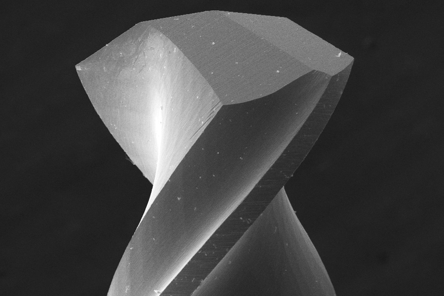
Fig. 1: SEM image of a drill tip after ultrasonic bath, oxygen plasma and etching

Fig. 2: Structure of the coatings
Deposition process
The coatings were deposited on a scia Coat 200 ion beam sputtering system. This system is specifically designed for coating substrates with a diameter of 200 mm, such as wafers. An argon plasma is generated in an ion beam source and accelerated as an ion beam onto the titanium target. For the multilayer, a titanium and a niobium target were placed on two positions of the target carousel and moved back and forth to switch between the materials. The sputtered material from the target is deposited as a uniform layer on the workpieces. The nitrogen required for the formation of TiN or NbN was added to the assist source as a reactive gas.
The study was carried out on 500 tungsten carbide tipped drill bits, each mounted on a specially developed substrate carrier with a magnetic holder and cleaned in an ultrasonic bath. The chamber was then loaded with the substrates and an oxygen plasma was used for further pre-cleaning. Before the actual coating, the drills were etched with an ion beam to improve the adhesion of the coating.
Results
The quality assessment of the coating performance was carried out by drilling holes in PCB composites and then analyzing the sections by the project partner KSG Leiterplatten. The ITW Chemnitz monitored the process reliability by measuring the layer thickness of the coated micro-drilling and milling tools. In addition, SEM images of the drills were made by Westsächsische Hochschule Zwickau.
Both coatings produced uniform layers with good adhesion, which showed no spalling even after increasing the stroke rate by a factor of 2 to 3 times. All quality criteria for the PCB product were fulfilled and verified 100 % in accordance with customer specifications and KSG requirements. By coating the tools, the tool life could be increased 2 to 3 times and thus the costs for new tools and storage capacities could be significantly reduced. In addition, machining times are reduced due to fewer tool changes during mechanical machining, improving overall productivity.
Conclusion
In summary, the utilization of dual ion beam sputtering for the deposition of nano wear resistant coatings has proven to be a pioneering solution for precision micro cutting tools. As the industry continues to drive miniaturization and demand higher performance tools, these advanced coatings are opening the way for increased productivity, reduced costs and improved manufacturing processes. Through continued research and collaboration, further advances in coating technology can be made, providing new opportunities for the application of nanocoatings in a variety of fields.
Project Partners:

Fig. 3: Principle of Dual Ion Beam Sputtering

Fig. 4: SEM image of a drill with TiN coating after 2020 drills
Related Information
Related Products: scia Coat 200
- In-situ change of coating materials due to rotational target holder with up to 5 water-cooled targets
- Controlled multilayer deposition based on process recipe
- Process monitoring with quartz crystal oscillator and/or optical thickness monitor (OTM) and test glass changer
- Direct wafer handling or adaptation to variable substrate sizes with carrier handling
Reach out
Please contact us for further information.
Any questions left?
scia Systems GmbH
Clemens-Winkler-Str. 6c
09116 Chemnitz
Germany
