Latest Company News

Ion beam technology from scia Systems pushes the development of China's semiconductor industry

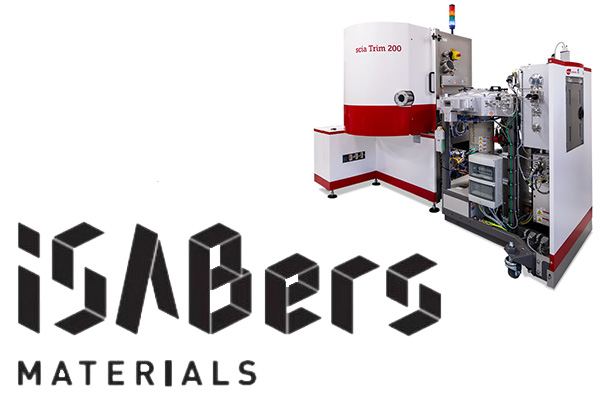
Founded in 2022, the Chinese company TJ Innovative Semiconductor Substrate Technology Co., Ltd. (ISST) has entered the market as a supplier of heterogeneous integration technologies for the semiconductor industry. For its new expansion plans and its new production lines ISST has now purchased a scia Trim 200. With this system, the surface of the substrate material can be processed ultra-precisely by ion beam trimming, so that layer thickness uniformities down to the atomic level of 0.1 nm can be achieved. ..

Read more
scia Trim 200 for ISABERS

Runxin MEMS Technologies increases output yield of produced filters by ion beam trimming

In March 2022, Runxin MEMS Technologies Co., Ltd. was established in the Microelectronics Science Park as a new industrial base for MEMS production in the Nanchang High tech Zone. The company now expands its capacities by purchasing a scia Trim 200. With this ion beam trimming system especially the production of BAW and SAW filters will be more efficient. By layer thickness trimming, the yield of functional components can be increased up to 90%...

Read more
Runxin MEMS Logo

scia Mill 200 starts its Journey to Chinese Cutting-Edge Technology

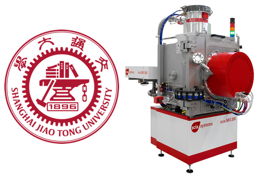
scia Systems is happy to announce the purchase of our ion beam etching system scia Mill 200 by another top C9 university of China: the Shanghai Jiao Tong University. It was founded in Shanghai in 1896 and has a long history in engineering and managerial sciences. With around 40,000 students the university offers opportunities in nine major disciplines: economics, law, literature, science, engineering, agriculture, medicine, management and arts.

scia System will support the university in its goal of becoming a "comprehensive, innovative and international" world-class university by supplying an ion beam etching tool with highest flexibility.

Read more
Logo SJTU with scia Mill 200

RWTH Aachen expands its microelectronics research laboratory for 2D electronics with an ion beam processing system scia Coat 200

With more than 47,000 students, the Rheinisch-Westfälische Technische Hochschule (RWTH) Aachen is the second largest university for technical courses in Germany. Their research laboratory will demonstrate the feasibility of large-scale fabrication of 2D layers. These consist of individual atomic layers of intrinsically stable crystals and can be stacked on top of each other - despite their different characteristics - and built up into complex (hetero) layer structures. The equipment required for this  will be set up in the Central Laboratory for Micro- and Nanotechnology and will now be completed by a scia Coat 200.

Read more
RWTH Aaachen Logo

Improved silicon wafer processing for ESA’s X-ray observatory "Athena"

With the Athena project, the European Space Agency will launch the largest X-ray telescope ever built into space. A new kind of optics had to be invented in order to achieve the goal of looking deeper into the universe than any previous X-ray observatory missions. scia Systems, a high-tech company based in Chemnitz, Germany, supplies crucial technology to produce these optics.

Read more

SPO module

New Application Note: Deposition of GMR Sensors on Large Areas

Magnetic field sensors for flexible and wearable devices are the key technology for motion detection, e.g. in industrial robotics, prosthetics, and virtual and augmented reality applications.

Sensors based on the giant magnetoresistance (GMR) effect can be printed on polymer films with a material thickness of 1 μm to 150 μm using a polymer carrier.

This GMR technology places high demands on a coating system. For instance, GMR stacks, which usually consist of multiple Co and Cu layers about 1 nm thick (Fig. 1), require an accuracy of the layer thickness of better than 0.1 nm. In our new Application Note, we provide an insight into the production of this sensors.

Learn more.


App-Note

Ion Beam Trimming System for Silex Microsystems in China

Silex Microsystems, the world's largest pure-play MEMS foundry, is expanding its facility in Beijing, China. Recently, a scia Trim 200 was commissioned there, a high-volume production system for precise surface correction of wafers up to 200 mm.

The tool is used to produce filters by local ion beam trimming, which are needed for high frequency technology, for example in WLAN or mobile communication.

Besides this first system, which is now handed over to production, two other tools will be installed in Silex over the next months. We are looking forward to a successful partnership!
silex microsystems Logo

Commitment 2022: scia Systems donates 2000 Euro to local projects

Every year, scia Systems sponsors up to four non-profit organizations or social projects suggested by its employees. Once again, the jury had a hard time choosing between all the projects. In addition to sports clubs, two social institutions were also able to prevail this year...

Read more
Our Engagement 2021

Apprentices wanted!

For apprenticeships starting in 2022, we are still looking for trainees in various fields, e.g. as Fachinformatiker/-in, Elektroniker/-in and Mechatroniker/-in. Do you have a preference for technology and good mathematics and physics knowledge? Then have a look on our open training positions. We offer exciting apprenticeship opportunities and very good chances to become hired after successful final examinations.

With the Bildungs-Werkstatt Chemnitz and its modern and qualified educational offerings, we have found a strong partner for our apprenticeship. Through the cooperation in the joint apprenticeship, we can not only convey all educational contents to our trainees, according the Vocational Training Act, but also continuously improve the quality of our apprenticeship today and in the future.

We look forward to continuing our successful cooperation.

scia Systems is one of the partners in the joint project for 3-nanometer microelectronics research "PIn3S"

The PIn3S project focuses on the development of process and equipment technology for the production of adaptive optics, which are required for semiconductor technology with conduction path distances of only 3 nanometers. We are proud to contribute our know-how and experience in ion beam and plasma technology to this project ...

Read more
Pin3S